Method of manufacturing a semiconductor device

Inactive Publication Date: 2005-04-21
RENESAS ELECTRONICS CORP
View PDF5 Cites 16 Cited by
  • Summary
  • Abstract
  • Description
  • Claims
  • Application Information

AI Technical Summary

Benefits of technology

[0032] Main advantageous effects which are brought about by the present invention are: red

Problems solved by technology

Therefore, the following problem may occur: foreign matter adhering to the semiconductor device's mounting surface, as mentioned abo

Method used


Image

  • Method of manufacturing a semiconductor device
  • Method of manufacturing a semiconductor device
  • Method of manufacturing a semiconductor device

Examples


Example

(First Embodiment)

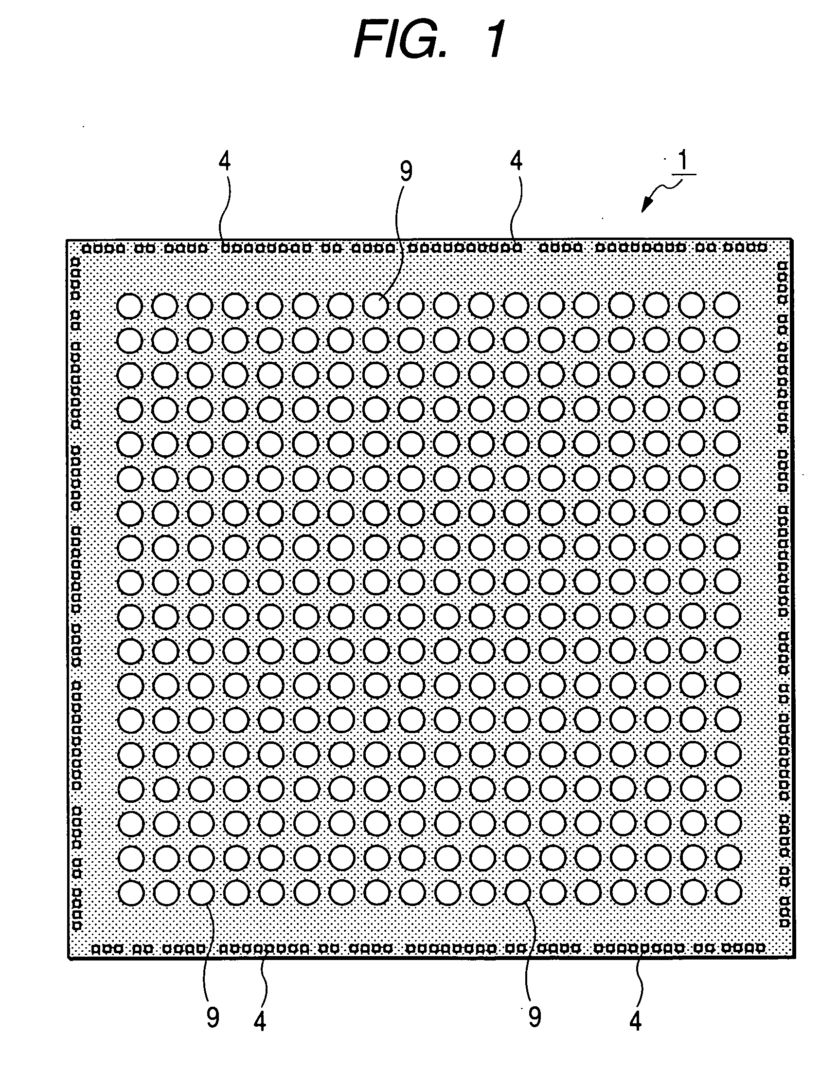
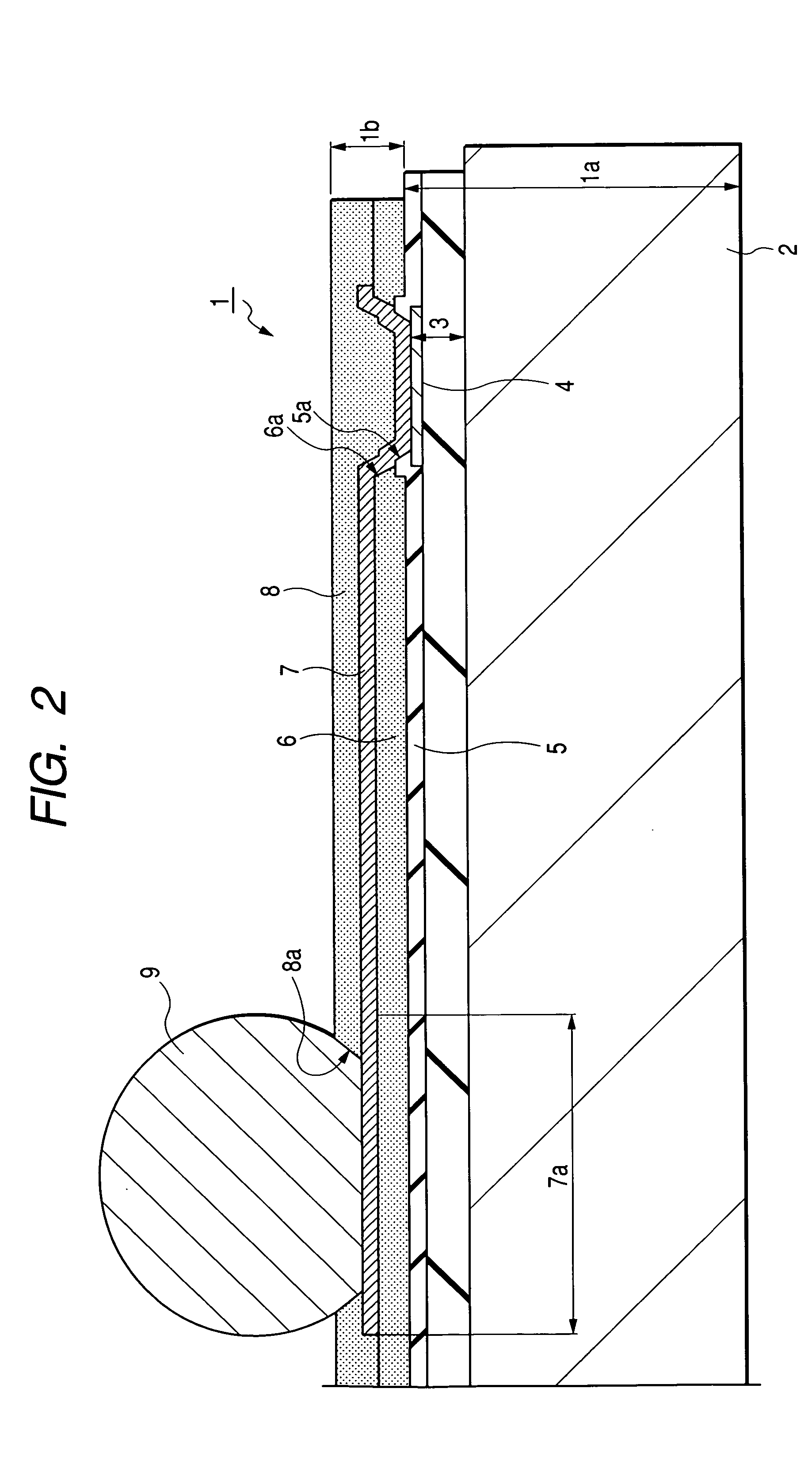
[0064] The first embodiment concerns a wafer level CSP type semiconductor device to which the present invention is applied. FIG. 1 is a plan view showing the mounting surface of a semiconductor device according to this first embodiment of the present invention; FIG. 2 is a sectional view showing the internal structure of a semiconductor device according to the first embodiment of the present invention; FIG. 3 is a plan view showing a wiring pattern on the mounting surface of a semiconductor device according to the first embodiment of the present invention; FIG. 4 is a flowchart showing the process of manufacturing a semiconductor device according to the first embodiment of the present invention; FIG. 5 is a plan view showing a semiconductor wafer used in the manufacture of a semiconductor device according to the first embodiment of the present invention. FIG. 6 to FIG. 13 illustrate steps in the manufacture of a semiconductor device according to the first embodim...

Example

(Second Embodiment)

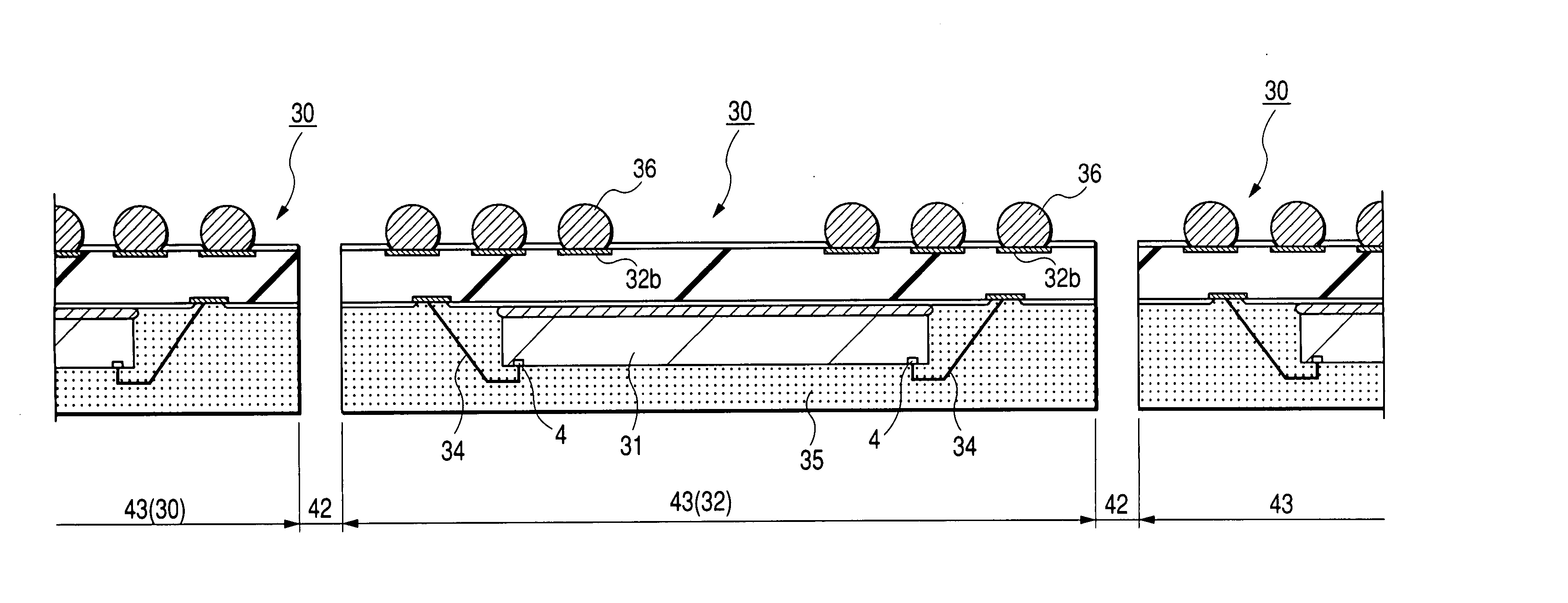
[0103] The second embodiment is directed to a chip level CSP type semiconductor device to which the present invention is applied.

[0104]FIG. 20 is a sectional view showing the internal structure of a semiconductor device according to a second embodiment of the present invention; FIG. 21 is a plan view showing the mounting surface of a semiconductor device according to the second embodiment of the present invention; FIG. 22 is a plan view showing a wiring pattern on the mounting surface of a semiconductor device according to the second embodiment of the present invention FIG. 23 is a plan view showing a multi-device substrate used in the manufacture of a semiconductor device according to the second embodiment of the present invention; FIG. 24 is a sectional view of the multi-device substrate in FIG. 23; FIG. 25 is a flowchart showing the process of manufacturing a semiconductor device according to the second embodiment of the present invention; and FIGS. 26 to 30...


PUM


Abstract

A method of manufacturing a semiconductor device involves the steps of: forming a plurality of product formation areas each having a circuit and a plurality of first electrode pads over a main surface of a semiconductor wafer; arranging a plurality of second electrode pads with larger pitches than the first electrode pads in each of the product formation areas; segmenting the semiconductor wafer to separate the plural product formation areas and provide a plurality of semiconductor devices each having the circuit, the plural first electrode pads and the plural second electrode pads on a first surface; and cleaning foreign matter off the first surface of the semiconductor device after the step of segmenting the semiconductor devices.

Description

CROSS-REFERENCE TO RELATED APPLICATION [0001] The present application claims priority from Japanese patent application No. 2003-340741, filed on Sep. 30, 2003, the content of which is hereby incorporated by reference into this application. BACKGROUND OF THE INVENTION [0002] The present invention relates to semiconductor device manufacturing technology. [0003] In connection with semiconductor devices of the type incorporated in small size electronic equipment, such as mobile phones, personal digital assistants and mobile personal computers, there is a demand for thin models, compact models and multi-pin models. As an example of semiconductor devices which meet such a demand, CSP (Chip Size Package) type devices are known. Various types of CSP type semiconductor devices have been proposed and commercialized. One of them is a CSP type semiconductor device which is manufactured using wafer packaging technology which combines wafer processing and a package assembly process (hereinafter c...

Claims


Application Information

Patent Timeline
IPC IPC(8): H01L23/52B08B7/00H01L21/00H01L21/30H01L21/3205H01L21/44H01L21/48H01L21/50H01L21/56H01L21/60H01L21/66H01L23/12H01L23/31H01L23/495
CPCH01L2924/01029H01L2924/01033H01L2924/01047H01L2924/01078H01L2924/01079H01L2924/01082H01L2924/14H01L2924/15311H01L2924/19043H01L2924/30105H01L2924/3011H01L21/4803H01L23/3114H01L23/3128H01L24/97H01L2224/32225H01L2224/48227H01L2224/73265H01L2224/97H01L2924/01013H01L24/48H01L2924/01005H01L2924/01006H01L2924/01019H01L2924/014H01L2224/45144H01L2924/12041H01L2224/85H01L2224/83H01L2224/92247H01L2924/00H01L2924/00012H01L24/45H01L24/73H01L2224/023H01L2924/00014H01L2924/12042H01L2924/181H01L2224/05599H01L2924/0001H01L21/60
Inventor YAMAGUCHI, YOSHIHIKOFUJISHIMA, ATSUSHIOHTA, YUSUKE
Owner RENESAS ELECTRONICS CORP
Why Eureka
Try Eureka