Modularized probe head

a moduler and probe head technology, applied in the field of probe heads, can solve the problems of damage to the wafer under test and affect the testing, and achieve the effects of reducing the cost of photomasks, reducing the connection height, and facilitating rework

Active Publication Date: 2005-04-28
CHIPMOS TECH INC
View PDF5 Cites 7 Cited by
  • Summary
  • Abstract
  • Description
  • Claims
  • Application Information

AI Technical Summary

Benefits of technology

[0013] Therefore, according to the present invention the probing chip 40 having a plurality of first probing tips 41 is mounted on the active surface 21 of the silicon substrate 20, and the side electrodes 42 of the probing chip 40 is joined by solder material 32 with the contact pad 24 of the silicon substrate 20. Under this structure, the height difference between the flexible printed circuit 50 and the first probing tips 41 can be increased, and would not affect the tips of the first probing tips 41. Furthermore, the position of the first probing tip 41 of probing chip 40 can be defined using the same photo mask for the bonding pads, which is the passivation openings of the wafer under test, in order to reduce the cost of photomasks due to different positions of bonding pads of different wafers under test. Therefore, it does not need to redesign a new silicon substrate 10, that is, the silicon substrate 10 according to the present invention can be standardized and universal. While a wafer with various distribution positions of bonding pads or changing the dimension of bonding pads, it only necessary to join with the corresponding probing chip 40 on an universal silicon substrate 10, without redesigning another new probe head. Besides, the side electrodes 42 of the probing chip40 are joined with the silicon subst

Problems solved by technology

While the raised contact members on the active surface of interconnect substrate probing the electrodes of a wafer under test, however, these bonding wire or

Method used


Image

  • Modularized probe head
  • Modularized probe head
  • Modularized probe head

Examples


Embodiment Construction

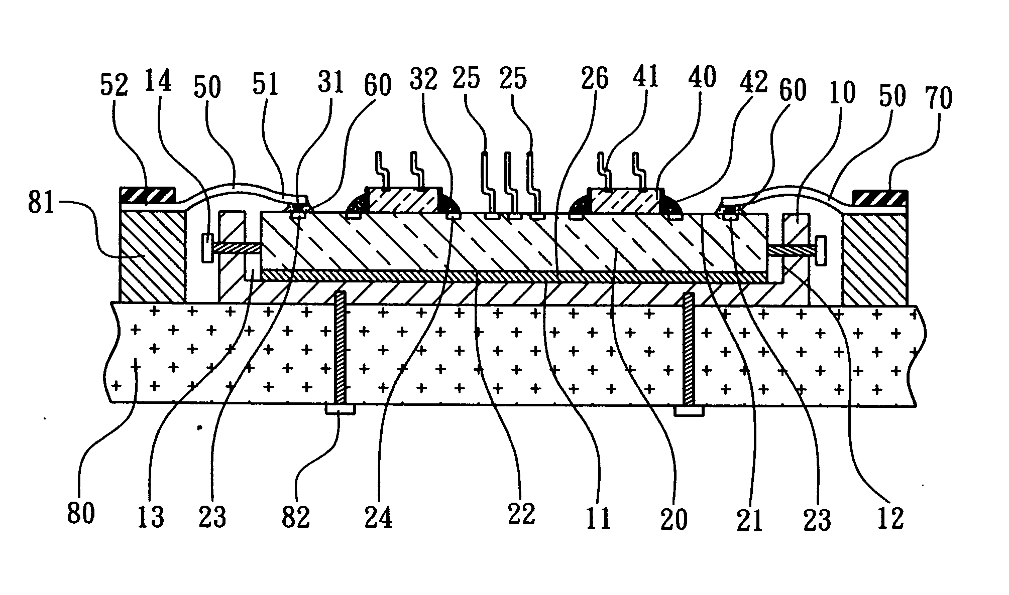
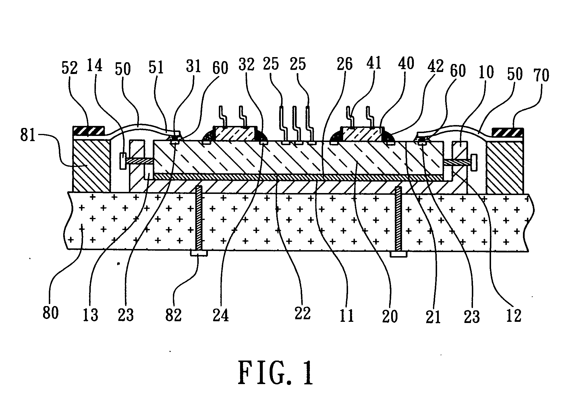
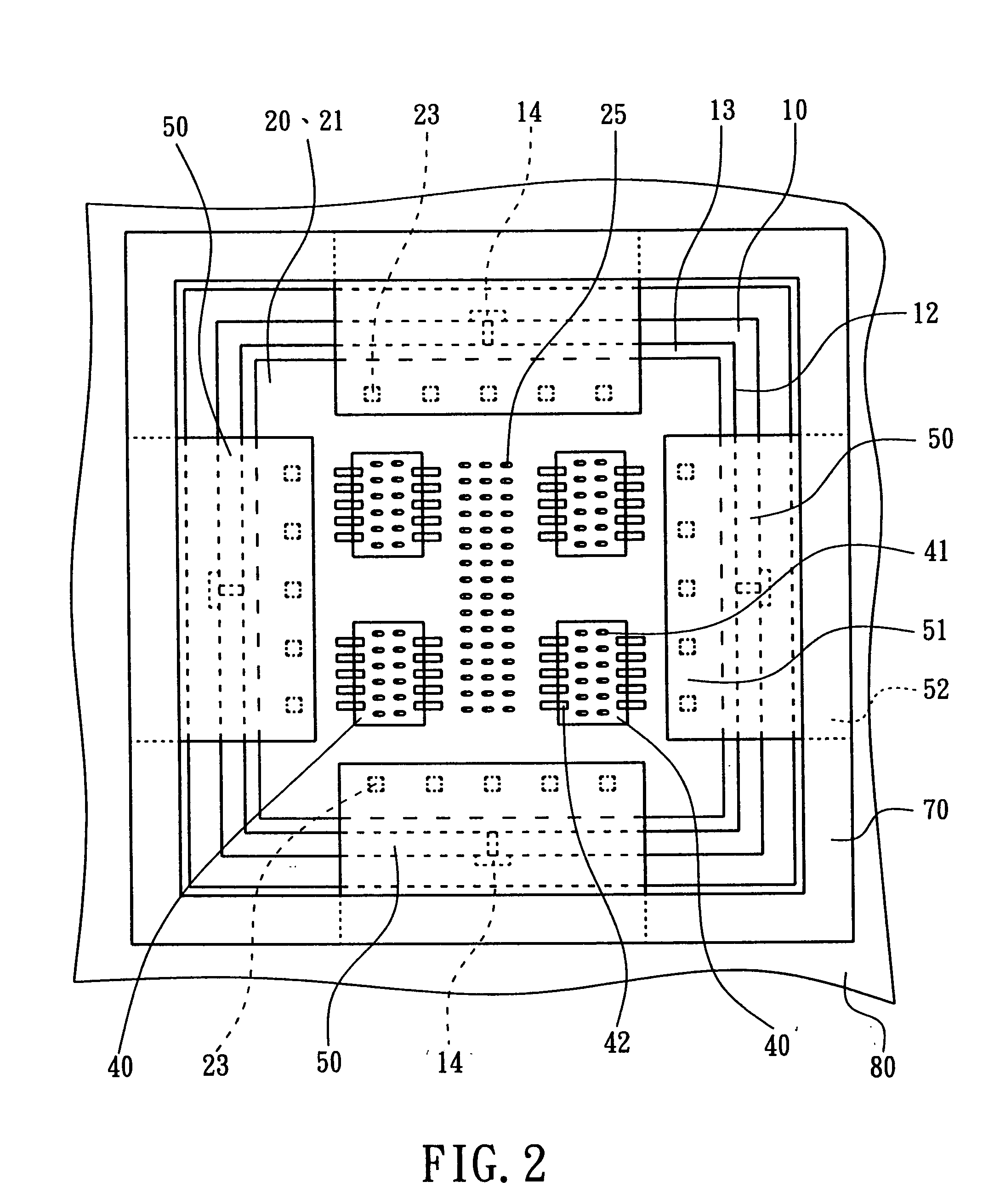
[0009] Please refer to the drawings attached, the present invention will be described by means of an embodiment below. According to the present invention, a modularized probe head mainly comprises a metal holder 10, a silicon substrate 20, at least a probing chip 40 and at least a flexible printed circuit 50, as shown in FIGS. 1 and 2, wherein the metal holder 10 is an alloyed metal holder, such as aluminum alloy. The metal holder 10 is a mechanically connecting base of the probe head for mounting with a multi-layer printed circuit board 80. The metal holder 10 has a bottom surface 11 and internal side surfaces 12 surrounding the bottom surface 11 for accommodating the silicon substrate 20.

[0010] The silicon substrate 20 is disposed on the metal holder 10. The silicon substrate 20 has same coefficients of thermal expansion as that of a wafer under test, and it can be fabricated to form test circuitry by semiconductor fabricating process. In this embodiment, the silicon substrate 20...


PUM


Abstract

A modularized probe head for modularly assembling on a probe card is configured for probing a semiconductor wafer under test. The probe head includes a silicon substrate having an active surface and an opposing back surface. The back surface of the silicon substrate is attached on a holder. The silicon substrate has a plurality of peripheral bond pads and contact pads on its active surface. At least a probing chip is mounted on the active surface of the silicon substrate. The probing chip has probing tips and side electrodes. The side electrodes are connected with the contact pads by means of solder material. The peripheral bonding pads of the silicon substrate are connected with a flexible printed circuit for electrically connecting to a multi-layer printed circuit board of a probe card.

Description

FIELD OF THE INVENTION [0001] The present invention relates to a probe head configured for assembling on a probe card for probing a semiconductor wafer under test. BACKGROUND OF THE INVENTION [0002] Conventionally, a probe head is assembled on a probe card for probing the semiconductor wafer under test. The conventional probe card comprises a probe head and a multi-layer printed circuit board shaped like a disk. Because the contact elements of probe head, such as probe needles or probing bumps, are required to contact the bonding pads of a wafer precisely, the precision and the matching of coefficient of thermal expansion of a probe head is higher than that of other probe card components. Therefore, the probe head is a key component of a probe card. [0003] A probe card with a probe head containing an interconnect substrate with raised contact members is disclosed in U.S. Pat. No. 6,359,456. The interconnect substrate is made of silicon by semiconductor fabricating process. Conductiv...

Claims


Application Information

Patent Timeline
IPC IPC(8): G01R31/28
CPCG01R31/2887
Inventor CHENG, S.J.LIU, AN-HONGWANG, YEONG-HERCHAO, YEONG-CHINGLEE, Y.J.
Owner CHIPMOS TECH INC
Why Eureka
Try Eureka