Mask data preparation

a mask data and mask technology, applied in the field of mask data preparation, can solve the problems of increasing the distortion in the pattern transfer process, creating problems, and printing small features on the wafer

Active Publication Date: 2005-04-28
APPLIED MATERIALS INC
View PDF5 Cites 41 Cited by
  • Summary
  • Abstract
  • Description
  • Claims
  • Application Information

AI Technical Summary

Problems solved by technology

As the feature size decreases, distortion in the pattern transfer process becomes more severe.
In the case of OPC, modifications of the design image account for optical limitations as well as mask fabrication limitations and resist limitations.
The destructive interference between adjacent regions of opposite phase creates a very sharp contrast at the boundary between the regions, thus leading to the printing of small features on the wafer.
The complexity of the correction after OPC can create some issue for vector-scan e-beam mask writing tool as very small slivers are created when the data is converted to the mask write tool format as shown in FIG. 3.
These small slivers lead to exposure dose inaccuracies when the mask is exposed which in turn result in dimension inaccuracies.
Another issue during the fracturing step is the difficulty to predict the shapes of the polygons created as illustrated in FIG. 4.
The difference in fracturing shapes will create some dosage difference between 403 and 406 when the photo-mask is exposed and it will result in dimension errors.
This problem can be even more acute in critical areas of the layout.

Method used


Image

  • Mask data preparation
  • Mask data preparation
  • Mask data preparation

Examples


Embodiment Construction

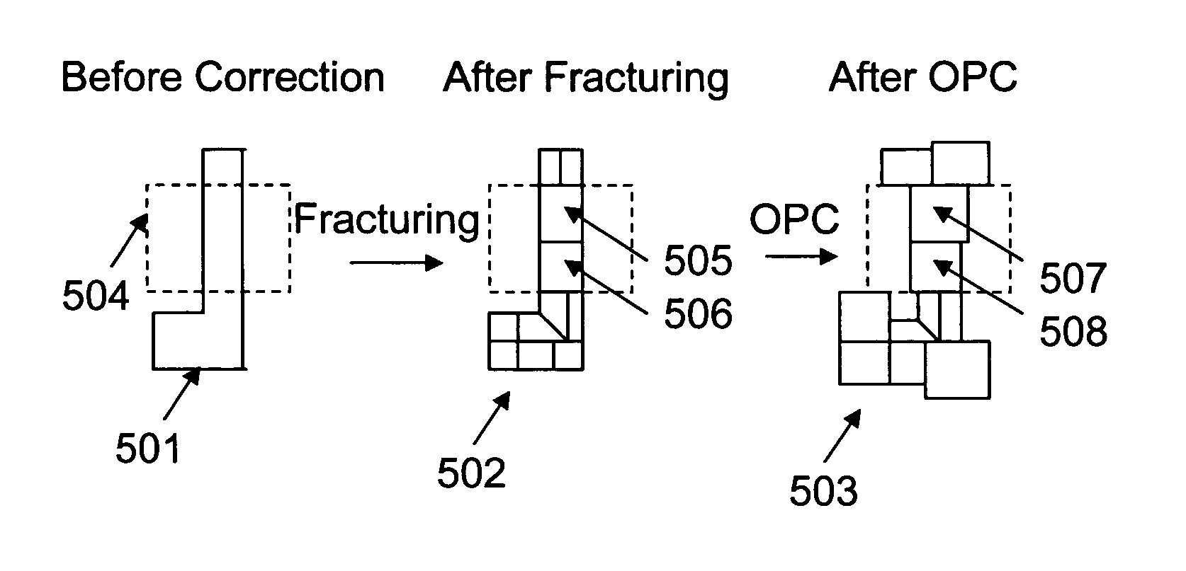
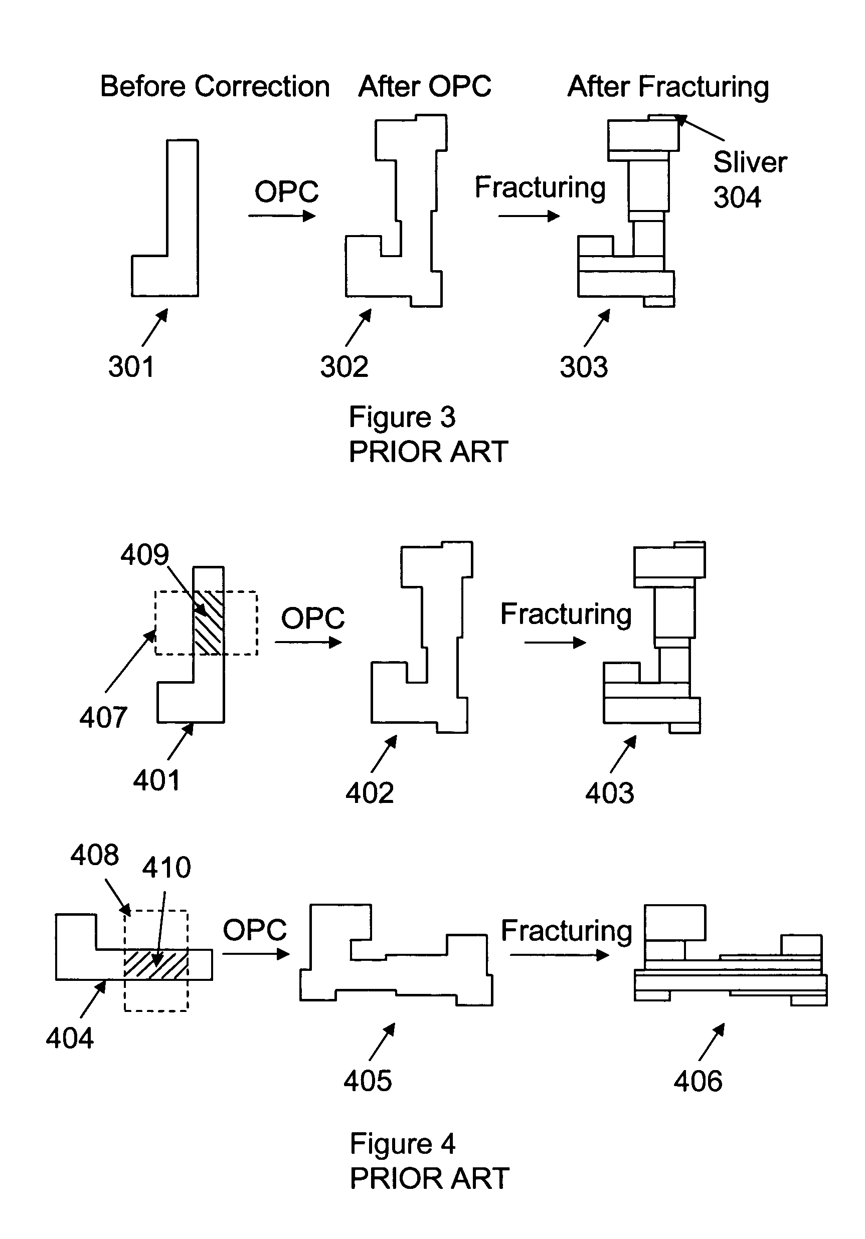
[0040] A technique described in FIG. 5 was developed to address the issues encountered during the fracturing of data for vector-scan mask writer. The polygon 501 before correction is first fractured in smaller shapes 502. Some of the edges of the shapes are abutting the original polygon. During the OPC step, the shapes are modified into 503 and no sliver was created as shown in FIG. 5. Fracturing into shapes before OPC presents some important advantages. First, the shapes can be chosen such that even with the largest OPC correction, the shape will not turn into a shape difficult to manufacture for the vector-scan e-beam mask writer. In FIG. 6a, 601 represents a shape after fracturing which is a part of a larger polygon 602 (not completely drawn on the figure). During the OPC step, the shape 602 could receive a maximum inner correction or a maximum outer correction as described in FIG. 6a. 603 represents the shape after maximum inner correction and 604 represents the shape after maxi...


PUM

PropertyMeasurementUnit
wavelengthsaaaaaaaaaa

Abstract

The manufacturing of integrated circuits relies on the use of optical proximity correction (OPC) to correct the printing of the features on the wafer. The data is subsequently fractured to accommodate the format of existing mask writer. The complexity of the correction after OPC can create some issues for vector-scan e-beam mask writing tools as very small slivers are created when the data is converted to the mask write tool format. Moreover the number of shapes created after fracturing is quite large and are not related to some important characteristics of the layout like for example critical areas. A new technique is proposed where the order of the OPC and fracturing steps is reversed. The fracturing step is done first in order to guarantee that no slivers are created and that the number of shapes is minimized. The shapes created can also follow the edges of critical zones so that critical and non-critical edges can be differentiated during the subsequent OPC step.

Description

FIELD OF THE INVENTION [0001] The invention relates to the process of fabricating semiconductor chips. More specifically, the invention relates to a method for preparing mask data. RELATED ART [0002] The high volume manufacturing of integrated circuits relies on the use of optical lithography to define the features printed on the semiconductor chips. The lithography process starts first by coating the surface of the semiconductor wafer with a material called resist. A source of radiation is then shone through the mask in the case of a transparent mask. For a reflective mask the radiation is reflected by the mask. The transparent mask is made of a substrate transparent to the radiation and coated with a patterned opaque layer defining clear and opaque regions to the radiation. Transparent masks are mostly used in optical lithography with typical wavelengths of 436 nm, 405 nm, 365 nm, 248 nm, 193 nm, and 157 nm. The reflective masks are made using a substrate reflective to the radiati...

Claims


Application Information

Patent Timeline
Patent Type & Authority Applications(United States)
IPC IPC(8): G03F1/14G06F17/50H01L
CPCG03F1/36G03F1/144G03F1/68
Inventor PIERRAT, CHRISTOPHEWONG, ALFRED K.
Owner APPLIED MATERIALS INC
Why Eureka
Try Eureka