Method and system for forming patterns using charged particle beam lithography
a technology of charged particle beam lithography and pattern formation, which is applied in the field of charge particle beam lithography to achieve the effect of reducing the cost of lithography
- Summary
- Abstract
- Description
- Claims
- Application Information
AI Technical Summary
Benefits of technology
Problems solved by technology
Method used
Image
Examples
Embodiment Construction
[0028]The present disclosure is related to lithography, and more particularly to the design and manufacture of a surface which may be a reticle, a wafer, or any other surface, using charged particle beam lithography.
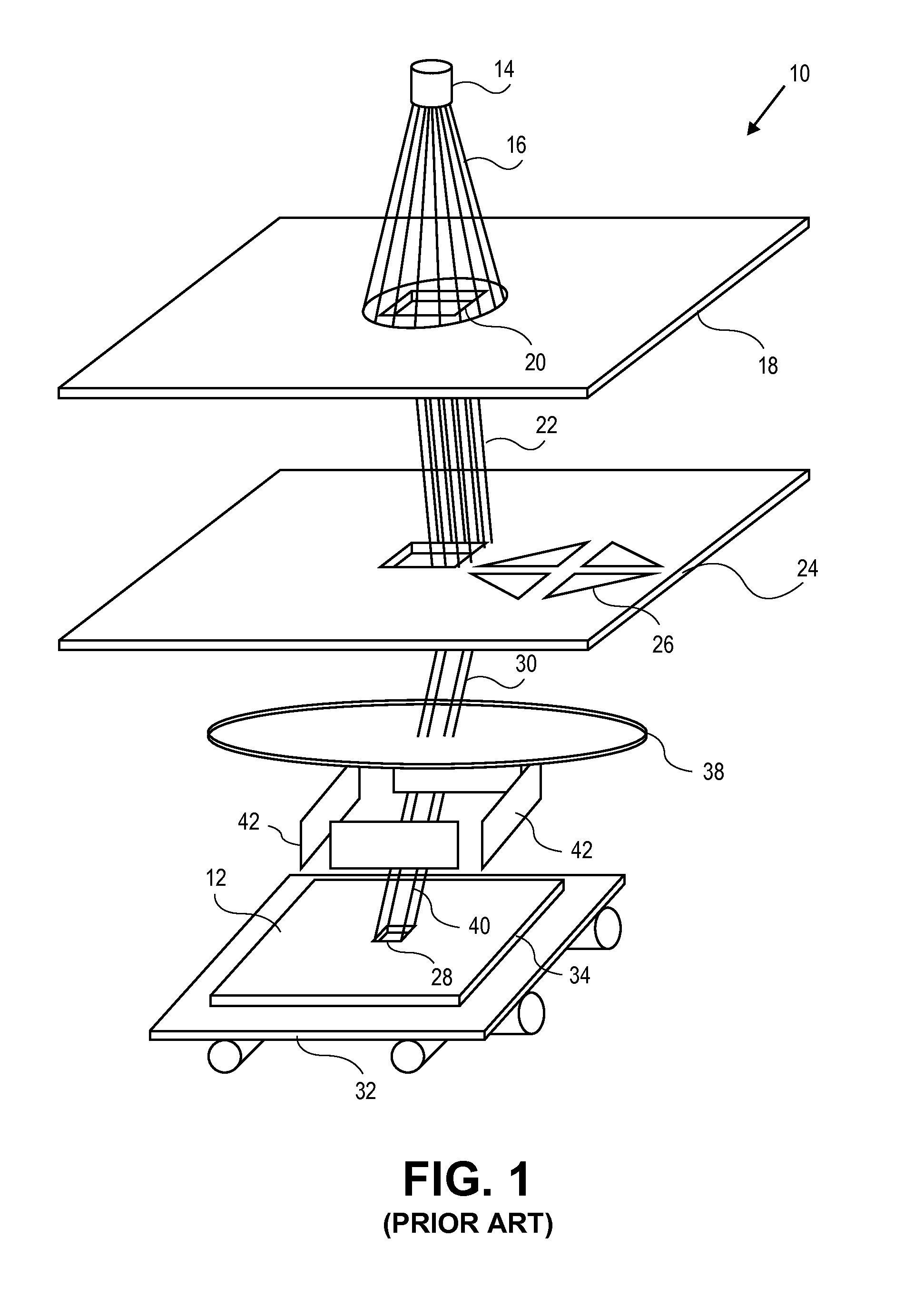
[0029]Referring now to the drawings, wherein like numbers refer to like items, FIG. 1 illustrates an embodiment of a lithography system, such as a charged particle beam writer system, in this case an electron beam writer system 10, that employs a variable shaped beam (VSB) to manufacture a surface 12. The electron beam writer system 10 has an electron beam source 14 that projects an electron beam 16 toward an aperture plate 18. The plate 18 has an aperture 20 formed therein which allows the electron beam 16 to pass. Once the electron beam 16 passes through the aperture 20 it is directed or deflected by a system of lenses (not shown) as electron beam 22 toward another rectangular aperture plate or stencil mask 24. The stencil 24 has formed therein a number of openings or ...
PUM
 Abstract
Description
Claims
Application Information


