Method and system for forming patterns with charged particle beam lithography

a technology of charged particle beam and pattern, applied in the field of semiconductor device production or manufacturing, can solve the problems of high computational cost, difficult to accurately translate the physical design to the actual circuit pattern developed on the resist layer, and difficult to add opc features, etc., to achieve the effect of reducing the sensitivity of the resulting pattern, reducing the sensitivity to changes in f, and reducing the sensitivity of the pattern

Active Publication Date: 2014-08-14
D2S
View PDF0 Cites 16 Cited by
  • Summary
  • Abstract
  • Description
  • Claims
  • Application Information

AI Technical Summary

Benefits of technology

[0016]A method for fracturing or mask data preparation or mask process correction for charged particle beam lithography is disclosed in which a plurality of shots are determined that will form a pattern on a surface, where shots are determined so as to reduce sensitivity of the resulting pattern to changes in βf. In some embodiments, the sensitivity to changes in βf is reduced by varying the charged particle surface dosage for a portion of the pattern.
[0017]Methods for forming patterns on a surface, and for manufacturing an integrated circuit are also disclosed, in which pattern sensitivity to changes in βf is reduced.

Problems solved by technology

An example of an end-use limitation is defining the geometry of a transistor in a way in which it cannot sufficiently operate at the required supply voltage.
The design rule limitations reflect, among other things, the smallest dimensions that can be reliably fabricated.
As the critical dimensions of the circuit pattern become smaller and approach the resolution value of the exposure tool, the accurate transcription of the physical design to the actual circuit pattern developed on the resist layer becomes difficult.
Adding OPC features is a very laborious task, requires costly computation time, and results in more expensive reticles.
Not only are OPC patterns complex, but since optical proximity effects are long range compared to minimum line and space dimensions, the correct OPC patterns in a given location depend significantly on what other geometry is in the neighborhood.
There are numerous manufacturing factors that also cause variations, but the OPC component of that overall error is often in the range listed.
Since these ideal ILT curvilinear patterns are difficult and expensive to form on a reticle using conventional techniques, rectilinear approximations or rectilinearizations of the curvilinear patterns may be used.
The rectilinear approximations decrease accuracy, however, compared to the ideal ILT curvilinear patterns.
However, because of the very high resolution of EUV, imperfections in a photomask, such as excessive line edge roughness (LER), will be transferred to the wafer.
Additionally, even though EUV mask shapes are not complicated by the addition of complex SRAFs or serifs required for conventional 193 nm lithography, EUV mask shapes are complicated by an addition of some complexities unique to EUV manufacturing.
In addition, since EUV processing of wafers is more expensive, it is desirable to reduce or eliminate multiple patterning.
In a world where overlapped or dose-modulated shots are used, sensitivity to beam blur or βf, which includes the physical effects of forward scattering, Coulomb effect and resist diffusion, can also be an issue.

Method used


Image

  • Method and system for forming patterns with charged particle beam lithography
  • Method and system for forming patterns with charged particle beam lithography
  • Method and system for forming patterns with charged particle beam lithography

Examples


Embodiment Construction

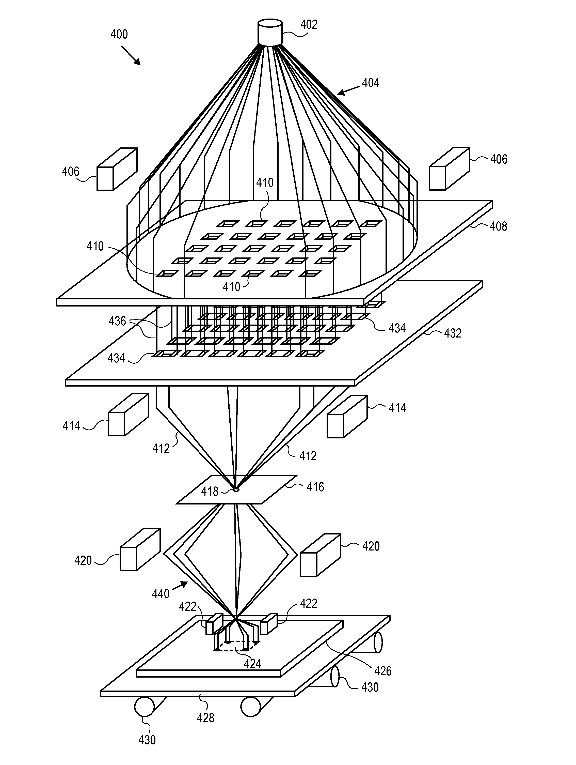
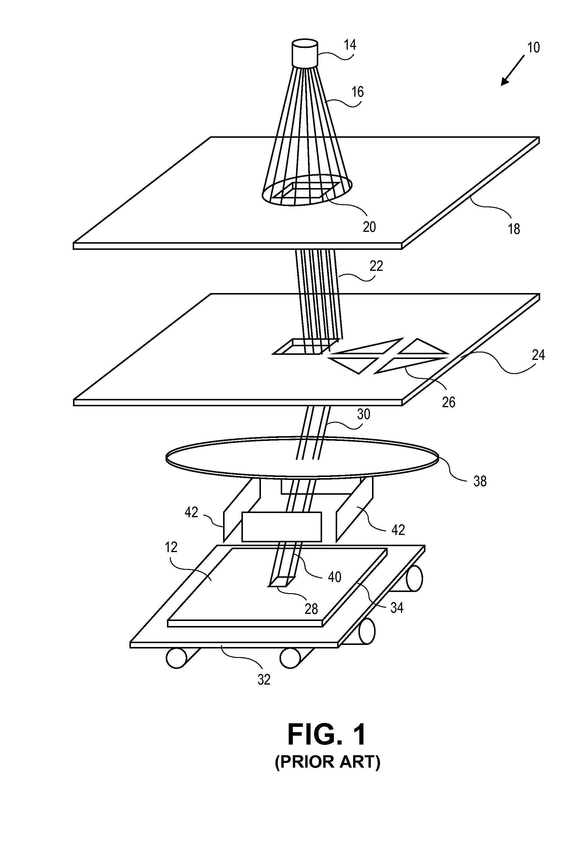
[0045]The present disclosure is related to lithography, and more particularly to the design and manufacture of a surface which may be a reticle, a wafer, or any other surface, using charged particle beam lithography.

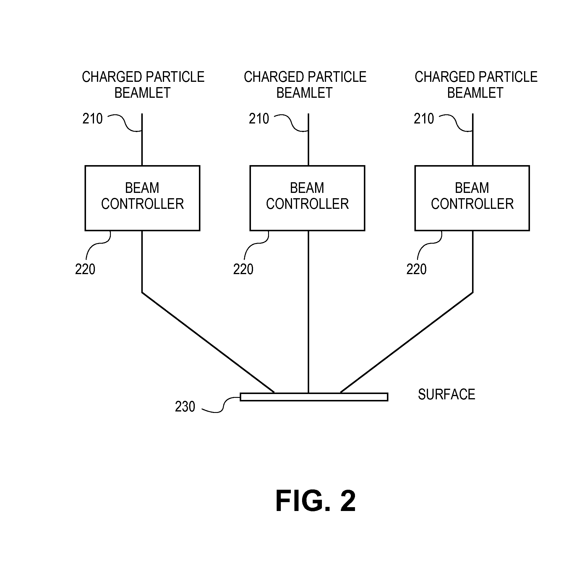
[0046]The improvements and advantages of the present disclosure can be accomplished by controlling the parameters of the shots forming a pattern, so as to reduce the magnitude of pattern variations caused by variation of βf, thereby allowing higher quality patterns to be formed on reticles and other surfaces such as wafers. In some embodiments, shot dosage, including multi-beam shot beamlet dosage, is varied to reduce sensitivity to changes in βf. In other embodiments, the amount of shot overlap in a plurality of shots may be controlled, either during initial shot determination, or in a post-processing step, to reduce sensitivity to changes in βf. In some embodiments, the sensitivity comprises pattern area sensitivity of the pattern formed on the surface. The reduced sen...


PUM


Abstract

In a method for fracturing or mask data preparation or mask process correction for charged particle beam lithography, a plurality of shots are determined that will form a pattern on a surface, where shots are determined so as to reduce sensitivity of the resulting pattern to changes in beam blur (βf). In some embodiments, the sensitivity to changes in βf is reduced by varying the charged particle surface dosage for a portion of the pattern. Methods for forming patterns on a surface, and for manufacturing an integrated circuit are also disclosed, in which pattern sensitivity to changes in βf is reduced.

Description

RELATED APPLICATIONS[0001]This application is a continuation-in-part of U.S. patent application Ser. No. 13 / 168,953 filed on Jun. 25, 2011 entitled “Method and System For Forming Patterns With Charged Particle Beam Lithography”, which is related to U.S. patent application Ser. No. 13 / 168,954 filed on Jun. 25, 2011 entitled “Method and System for Forming High Accuracy Patterns Using Charged Particle Beam Lithography”; both of which are hereby incorporated by reference for all purposes.BACKGROUND OF THE DISCLOSURE[0002]In the production or manufacturing of semiconductor devices, such as integrated circuits, optical lithography may be used to fabricate the semiconductor devices. Optical lithography is a printing process in which a lithographic mask or photomask manufactured from a reticle is used to transfer patterns to a substrate such as a semiconductor or silicon wafer to create the integrated circuit (I.C.). Other substrates could include flat panel displays, holographic masks, or ...

Claims


Application Information

Patent Timeline
Patent Type & Authority Applications(United States)
IPC IPC(8): G06F17/50
CPCG06F17/5068G03F1/78H01J37/3174H01J2237/31764H01J2237/31771H01J2237/31776Y10S430/143B82Y10/00B82Y40/00G03F1/20H01L21/027G06F30/20G06F30/398G03F7/2037G03F7/2063H01J37/147H01J37/3175
Inventor FUJIMURA, AKIRABORK, INGO
Owner D2S
Why Eureka
Try Eureka