In-pixel kTC noise suppression using circuit techniques

Active Publication Date: 2005-05-05
APTINA IMAGING CORP
View PDF7 Cites 37 Cited by
  • Summary
  • Abstract
  • Description
  • Claims
  • Application Information

AI Technical Summary

Benefits of technology

[0020] The present invention provides a circuit and method for reducing kTC noise in CMOS imagers while minimizing power dissipation. Correlated double sampling (CDS) is performed withi

Problems solved by technology

Doing so, however, can require deviating from a standard CMOS integrated circuit fabrication process, thereby further increasing the cost of manufacturing the image sensor circuit.
Some limitations on the above-described double sampling process do exist, however.
With r

Method used


Image

  • In-pixel kTC noise suppression using circuit techniques
  • In-pixel kTC noise suppression using circuit techniques
  • In-pixel kTC noise suppression using circuit techniques

Examples


Example

[0036] In the following detailed description, reference is made to the accompanying drawings which form a part hereof, and in which is shown by way of illustration specific embodiments in which the invention may be practiced. These embodiments are described in sufficient detail to enable those of ordinary skill in the art to make and use the invention, and it is to be understood that structural, logical or procedural changes may be made to the specific embodiments disclosed without departing from the spirit and scope of the present invention.

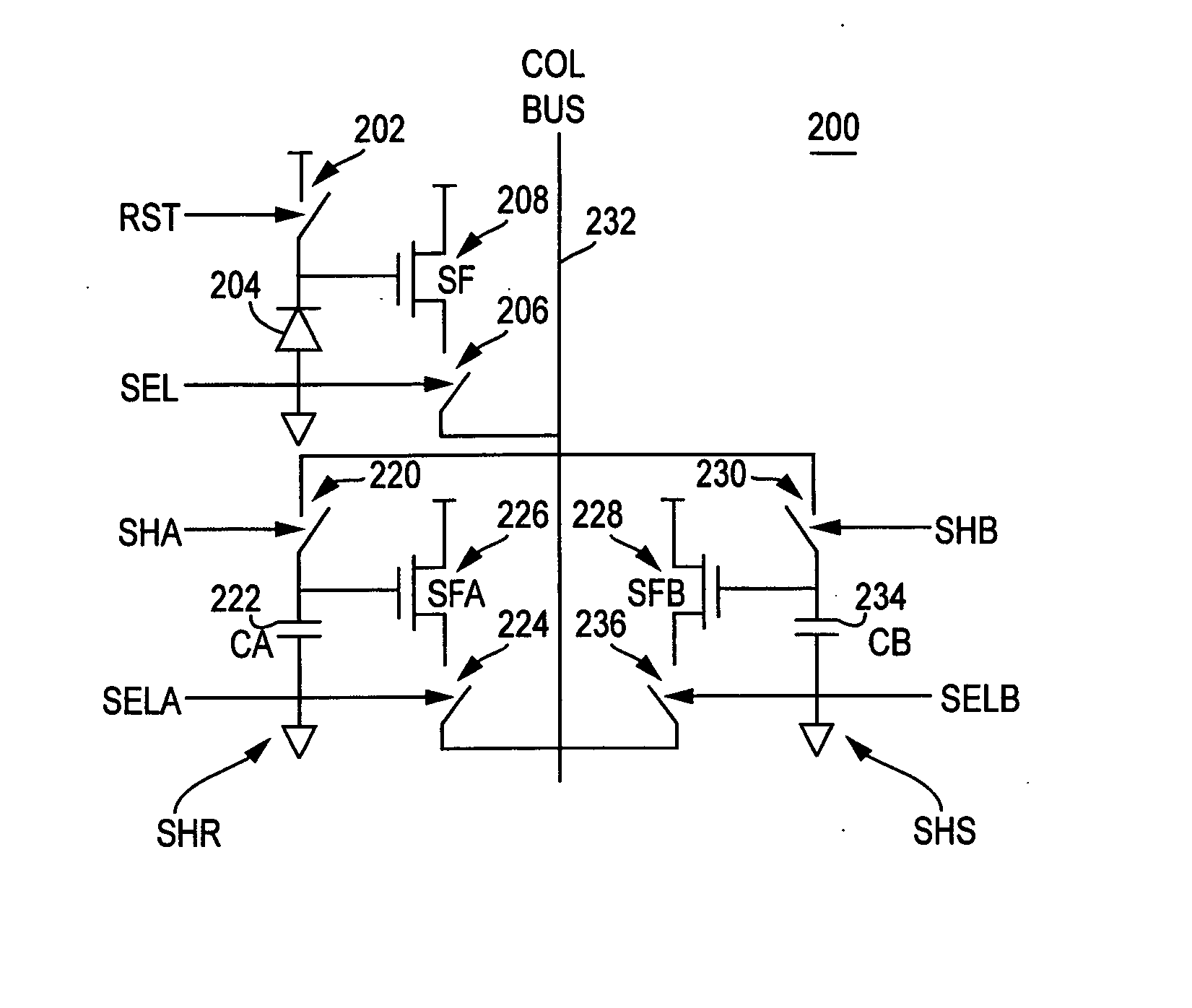
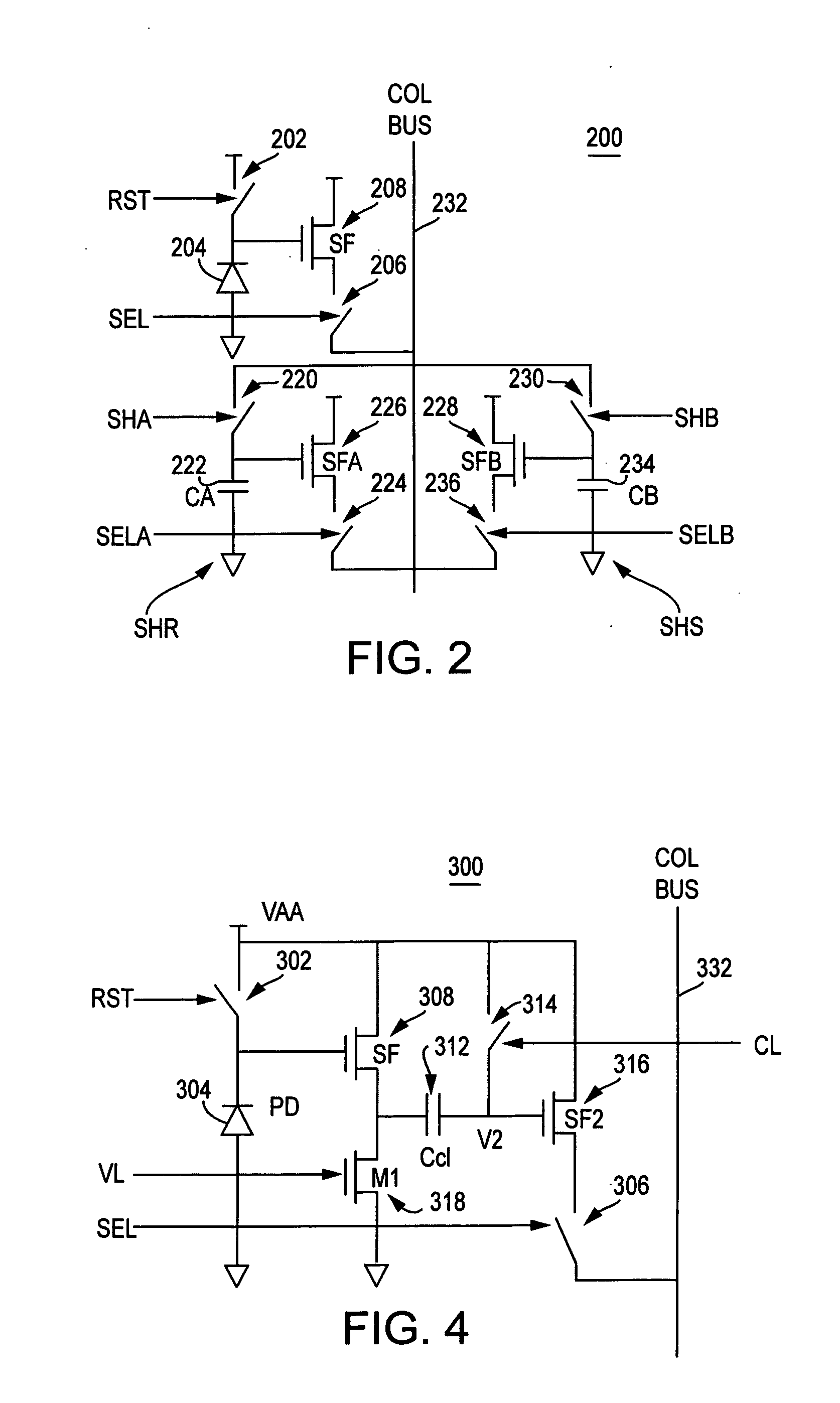
[0037]FIG. 2 depicts a schematic diagram of a pixel 200, in accordance with an exemplary embodiment of the invention. The pixel 200 consists of three sections. The upper section consists of a reset transistor 202, a photosensitive element (e.g., a photodiode) 204, a source-follower transistor 208 and a row select transistor 206 coupled to a column bus 232. The lower portion of the pixel 200 is made up of two sample and hold (SH) circuits.

[0038...


PUM


Abstract

A circuit and method for reducing kTC noise in CMOS imagers while minimizing power dissipation is disclosed. Correlated double sampling (CDS) is performed within each pixel such that the reset voltage and the integration voltage are sampled and stored within the pixel until the voltages are forwarded to a differential amplifier for subtraction.

Description

FIELD OF THE INVENTION [0001] The present invention relates generally to complementary metal oxide semiconductor (CMOS) imagers, and more particularly to kTC noise suppression circuits for use with CMOS imagers. BACKGROUND OF THE INVENTION [0002] Image sensors are used in a variety of different types of digital image capture systems, including products such as scanners, copiers, and digital cameras. The image sensor is typically composed of an array of light-sensitive pixels that are electrically responsive to incident light reflected from an object or scene whose image is to be captured. [0003] The performance of an image capture system depends in large part on the sensitivity of each individual pixel in the sensor array and its immunity from noise. Pixel sensitivity is defined here as being related to the ratio of a change in the pixel output voltage to the photogenerated charge in the pixel. Noise can be caused by a variety of known sources. An image sensor with increased noise i...

Claims


Application Information

Patent Timeline
IPC IPC(8): H01L27/00H04N5/363H04N5/3745
CPCH04N5/3575H04N5/363H04N5/3559H04N5/37452H04N5/378H04N5/374H04N25/59H04N25/616H04N25/65H04N25/771H04N25/76H04N25/75
Inventor FOSSUM, ERIC R.
Owner APTINA IMAGING CORP
Why Eureka
Try Eureka