Superconducting integrated circuit and methods of forming same

a superconducting integrated circuit and integrated circuit technology, applied in the direction of superconductor devices, electrical devices, semiconductor devices, etc., can solve the problems of limiting wide-scale adoption, inevitably losing energy, and heat dissipation, and the specialized nature of most superconducting materials

Inactive Publication Date: 2005-05-05
THE BOEING CO
View PDF16 Cites 14 Cited by
  • Summary
  • Abstract
  • Description
  • Claims
  • Application Information

AI Technical Summary

Benefits of technology

[0006] According to various exemplary embodiments, an integrated circuit formed on a substrate suitably includes a number of superconducting junctions. Each superconducting junction includes a first superconducting material disposed upon the substrate, an insulating material formed on the first superconducting material, and a second superconducting material formed on the insulating material to create a Josephson junction. The second superconducting material is a different material from the first superconducting material to aid in manufacturability. Any number of electrically conductive interconnects are also provided to interlink the superconducting junctions to thereby form the integrated circuit. Examples of superconducting materials that may be used for the various layers include YBaCu3O7-y (YBCO) and Bi2Sr2CaCu2Oy (Bi2212).

Problems solved by technology

When electricity flows in a conventional conducting material (e.g. copper wire), some energy is inevitably lost due to heat dissipation.
Although many have attempted to exploit Josephson currents in various devices and circuits, the specialized nature of most superconducting materials has limited wide-scale adoption, particularly within integrated circuits such as computer chips.
In particular, conventional Josephson devices are formed from two identical layers of superconducting material, which can be very difficult to process with conventional manufacturing techniques.
Photolithography used in semiconductor fabrication, for example, can be very difficult to apply to superconducting chips due to very precise requirements in forming multiple layers of a single superconducting material.

Method used


Image

  • Superconducting integrated circuit and methods of forming same
  • Superconducting integrated circuit and methods of forming same
  • Superconducting integrated circuit and methods of forming same

Examples


Embodiment Construction

[0014] The following detailed description of the invention is merely exemplary in nature and is not intended to limit the invention or the application and uses of the invention. Furthermore, there is no intention to be bound by any theory presented in the preceding background of the invention or the following detailed description of the invention.

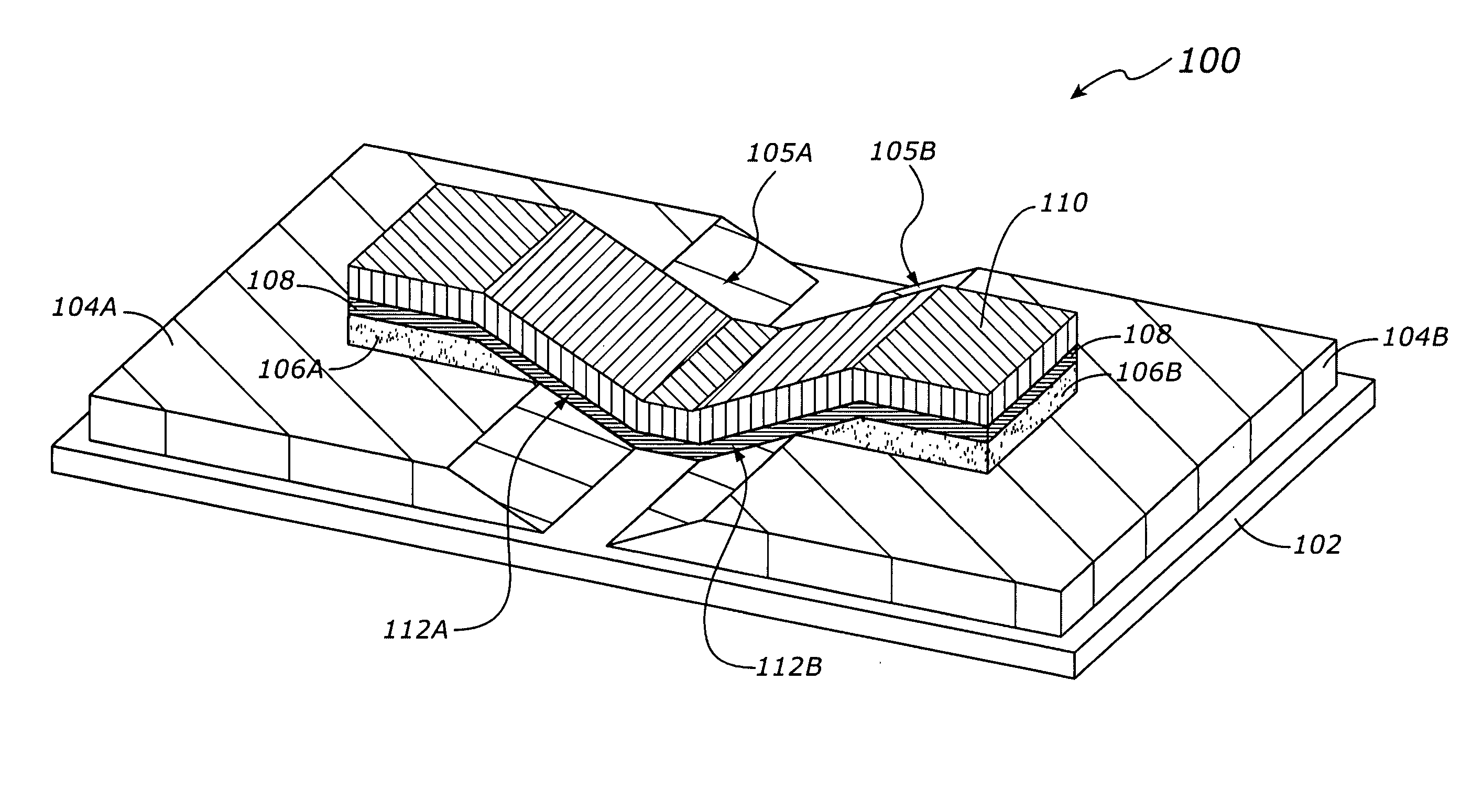
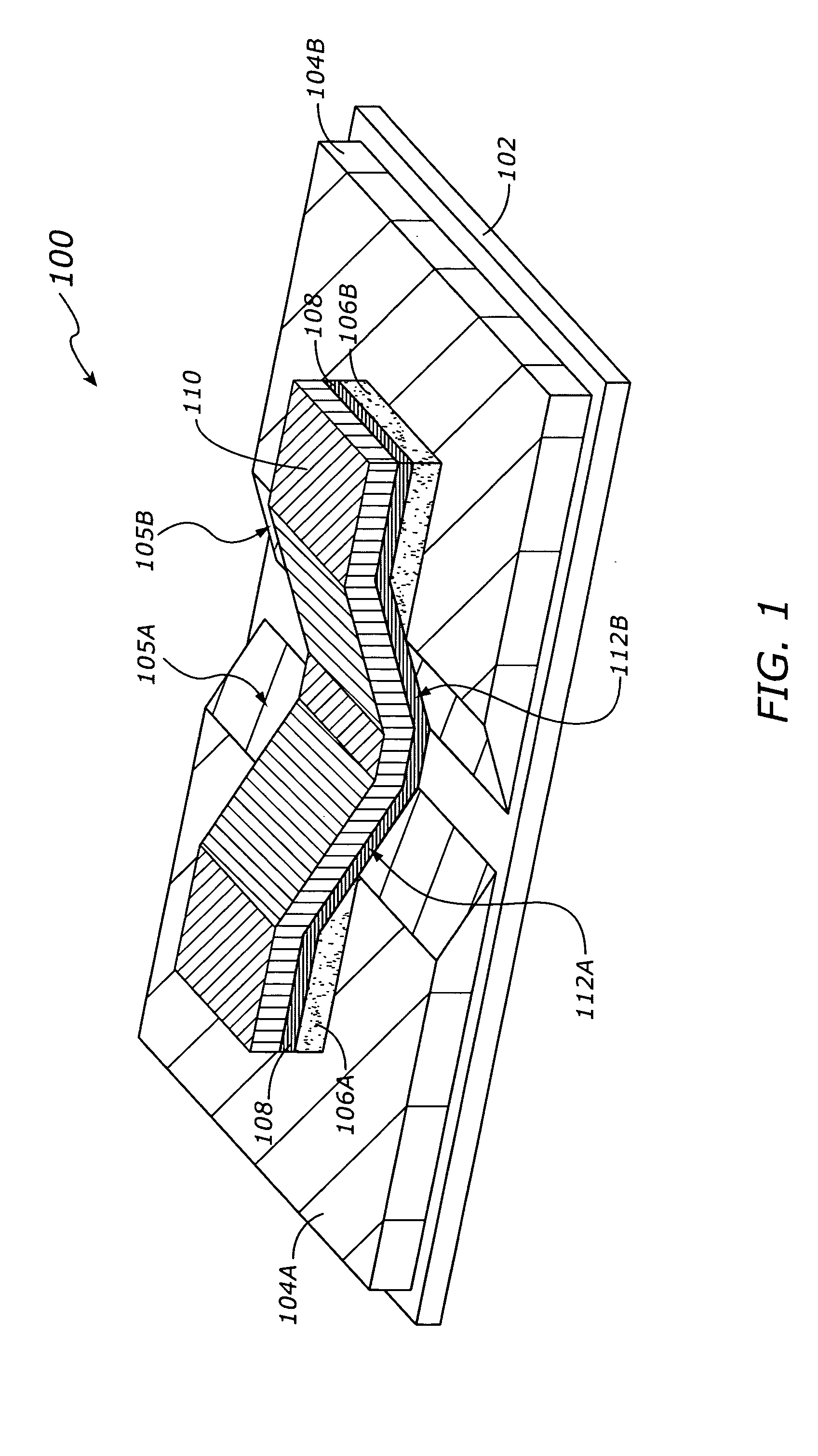
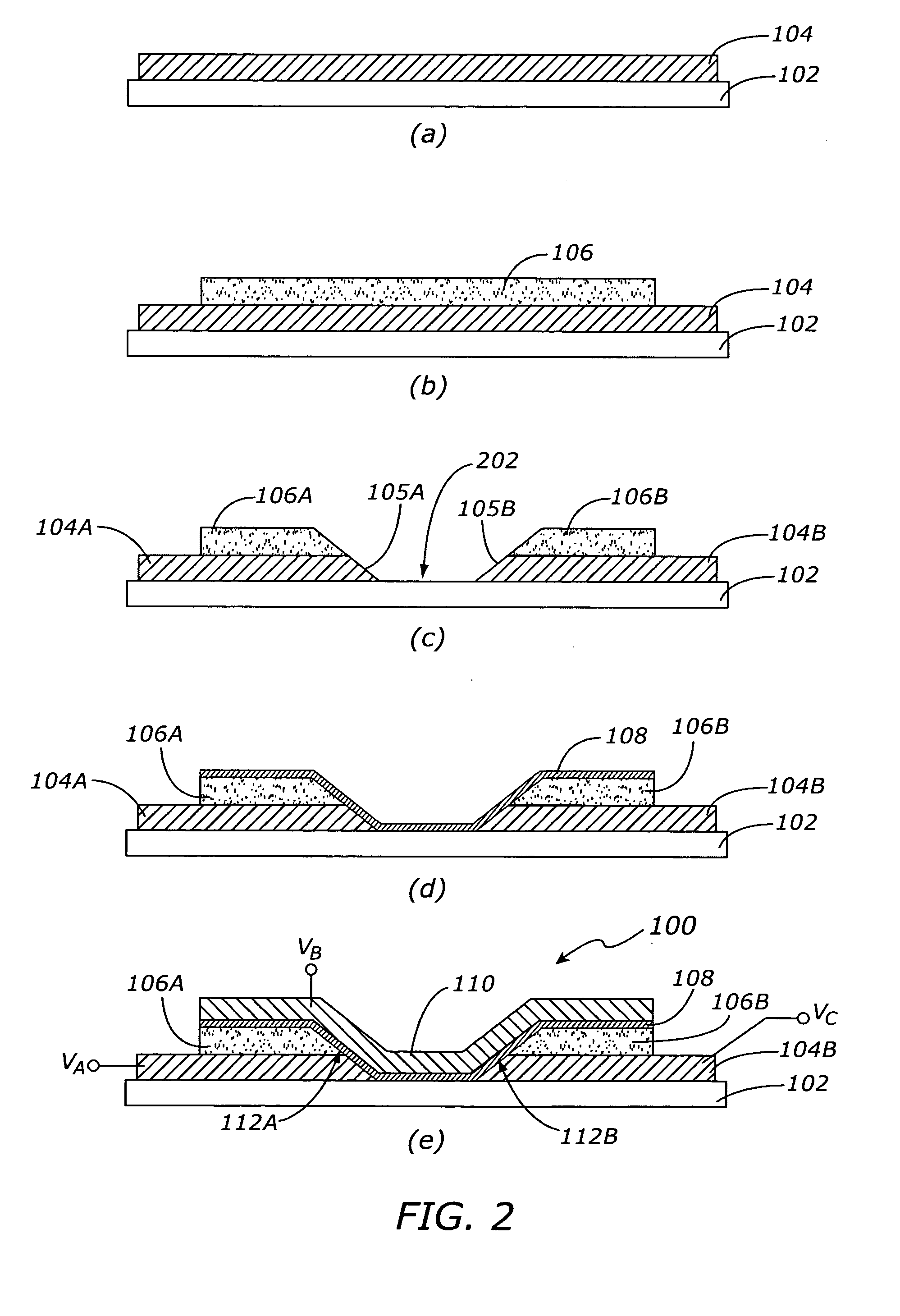
[0015] According to various exemplary embodiments, a superconducting integrated circuit suitably includes one or more Josephson junctions formed with non-identical layers of superconducting material. A first layer may be formed of YBaCu3O7-y (YBCO) and a second layer may be formed of Bi2Sr2CaCu2Oy (Bi2212), for example, to reduce the level of precision needed to etch or otherwise process the various materials on the integrated circuit. In a further embodiment, superconducting devices are formed with multiple Josephson junctions to create Josephson diodes, transistors or other devices. Such devices may be interconnected as appropriate to fo...


PUM


Abstract

An integrated circuit formed on a substrate suitably includes a number of superconducting junctions. Each superconducting junction includes a first superconducting material disposed upon the substrate, an insulating material formed on the first superconducting material, and a second superconducting material formed on the insulating material to create a Josephson junction. The second superconducting material is a different material from the first superconducting material to aid in manufacturability. Any number of electrically conductive interconnects are also provided to interlink the superconducting junctions to thereby form the integrated circuit. Examples of superconducting materials that may be used for the various layers include YBaCu3O7-y (YBCO) and Bi2Sr2CaCu2Oy (Bi2212). Various circuits and techniques relating to superconducting devices are also described.

Description

TECHNICAL FIELD [0001] The present invention generally relates to superconducting devices, and more particularly relates to an integrated circuit including superconducting devices. BACKGROUND [0002] When electricity flows in a conventional conducting material (e.g. copper wire), some energy is inevitably lost due to heat dissipation. Superconductors, however, are materials that conduct electricity without appreciable loss of energy when the material is cooled below a critical temperature (Tc). Critical temperatures vary among superconducting materials, but are typically on the order of 50-130 degrees Kelvin, or the approximate temperature of liquid helium or nitrogen. Because no heat is produced as electrons pass through the complex lattice structure of a superconducting material, superconductors are able to transfer electricity with no significant current loss during transmission. [0003] In addition to conducting electricity very efficiently, superconductors have been known to prod...

Claims


Application Information

Patent Timeline
Patent Type & Authority Applications(United States)
IPC IPC(8): H01L27/18H01L39/24
CPCH01L39/2496H01L27/18H10N69/00H10N60/0941
Inventor HUNT, JEFFREY H.
Owner THE BOEING CO
Why Eureka
Try Eureka