Display device and electronic device

a display device and electronic technology, applied in static indicating devices, instruments, semiconductor lamps, etc., can solve the problem of imposing space limitations on the placement of detour wirings, and achieve good balance in light-emitting brightnesses

Inactive Publication Date: 2005-05-05
SEMICON ENERGY LAB CO LTD
View PDF15 Cites 37 Cited by
  • Summary
  • Abstract
  • Description
  • Claims
  • Application Information

AI Technical Summary

Benefits of technology

[0028] In view of the above-mentioned problems, this invention provides an EL display device capable of producing a highly fine color display.
[0029] The present inventors have attempted to increase the widths of the detour wirings for those EL elements for which an increased current is to be supplied. Therefore, the wiring resistance of the detour wirings decreases for those pixels to which a large current is to be supplied. As the wiring resistance decreases, a drop of potential through the detour wirings decreases, and a large current can be supplied to the EL elements. In the practical panel, limitation is imposed on space for laying the detour wirings. By changing the ratio of widths of the detour wirings for each of the colors, therefore, it is allowed to maintain a balance in the magnitudes of currents flowing into the EL elements of each of the colors.
[0032] In this invention, further, the amplitude of the video signals may be increased only for those pixels whose EL elements are to be supplied with a large current. Owing to the above constitution, video signals of too large amplitudes need not be input to all of the pixels, and the consumption of electric power can be suppressed.
[0039] According to the above-mentioned constitution of the invention, the EL drive TFTs are suppressed from being deteriorated even when the current controlled by the EL drive TFTs has increased due to an increase in the absolute value of current flowing through the power source feed lines. It is further allowed to adjust the light-emitting brightness of the EL element relying on the voltage applied to the EL element and, hence, to display a picture of vivid colors maintaining a good balance in the light-emitting brightnesses of red color, blue color and green color.

Problems solved by technology

In the practical panel, limitation is imposed on space for laying the detour wirings.

Method used


Image

  • Display device and electronic device
  • Display device and electronic device
  • Display device and electronic device

Examples


embodiments

Embodiment 1

[0070] In this embodiment, the amplitude of the digital signals is increased for those pixels that require large voltages for the EL elements.

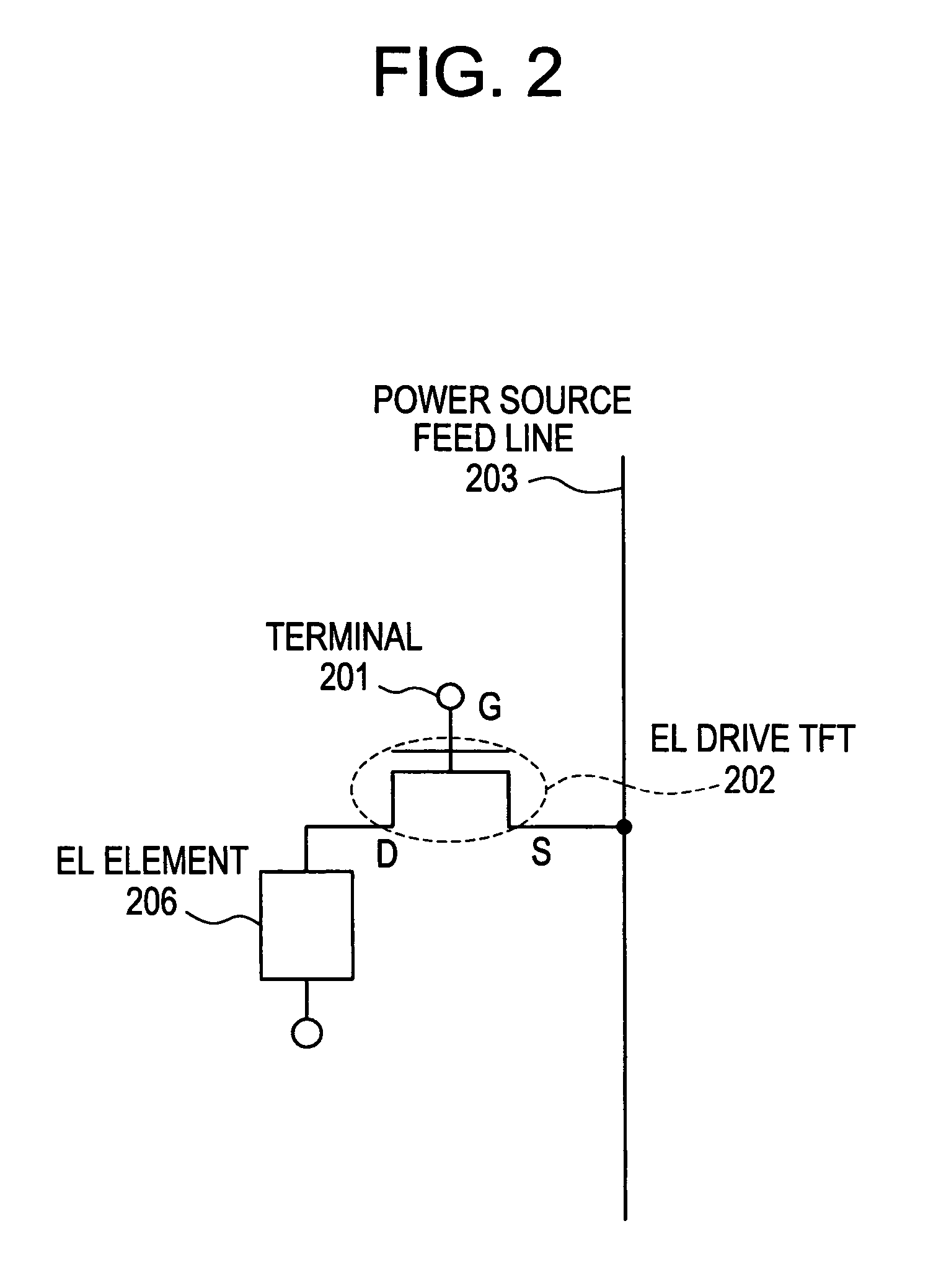
[0071]FIG. 2 schematically illustrates the constitution of connection between the EL drive TFT and the EL element in the pixel in the EL display device, and wherein reference numeral 202 denotes an EL drive TFT, 203 denotes a power source feed line, and 206 denotes an EL element. The gate electrode of the EL drive TFT 202 receives a digital signal that is given to a terminal 201. The source region of the EL drive TFT 202 is connected to the power source feed line 203, and the drain region thereof is connected to a pixel electrode possessed by the EL element 206.

[0072] If the absolute value of the current given to the power source feed line 203 is increased to increase the light emitting brightness of the EL element, the off current of the EL drive TFT 202 (current that flows in a state where the TFT is turned off) increases. The...

embodiment 2

[0075] This embodiment deals with a concrete constitution of the source signal line drive circuit used in the embodiment 1.

[0076]FIG. 3 is a block diagram of a source signal line drive circuit according to this embodiment, and wherein reference numeral 400 denotes a pixel unit, and 401 denotes a source signal line drive circuit. The source signal line drive circuit 401 includes a shift register circuit 402, a first latch circuit 403, a second latch circuit 404, a level shifter circuit 405 and a buffer circuit 406.

[0077] A digital signal (DV) is input to the first latch circuit 403 from the outside of the source signal line drive circuit 401 and is held therein according to a timing signal (TS) formed by the shift register circuit 402. When the digital signals of all bits are input and held in the first latch circuit 403, the digital signals held in the first latch circuit 403 are input to the second latch circuit 404 at one time and are held therein according to a latch pulse (LP)...

embodiment 3

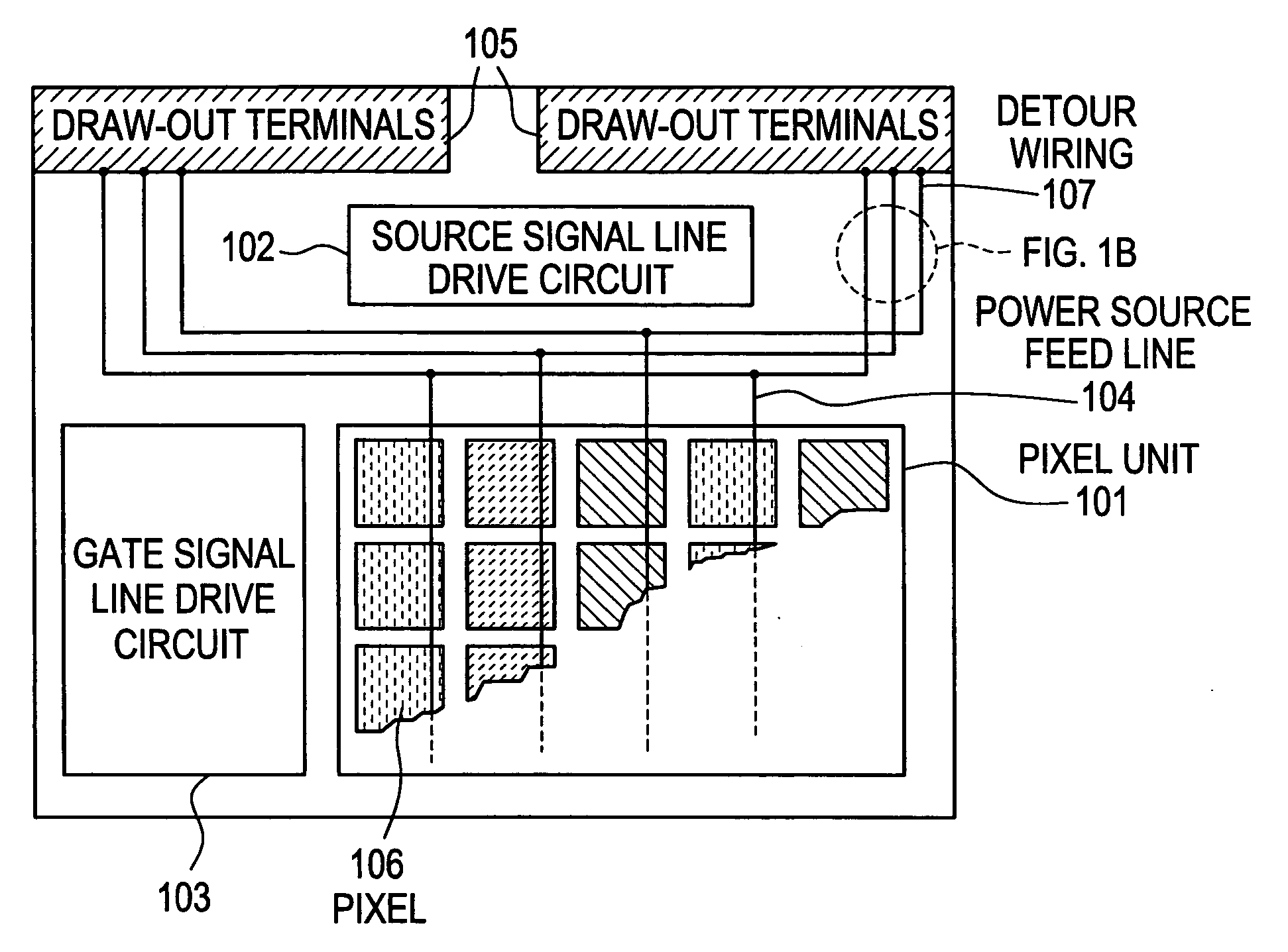
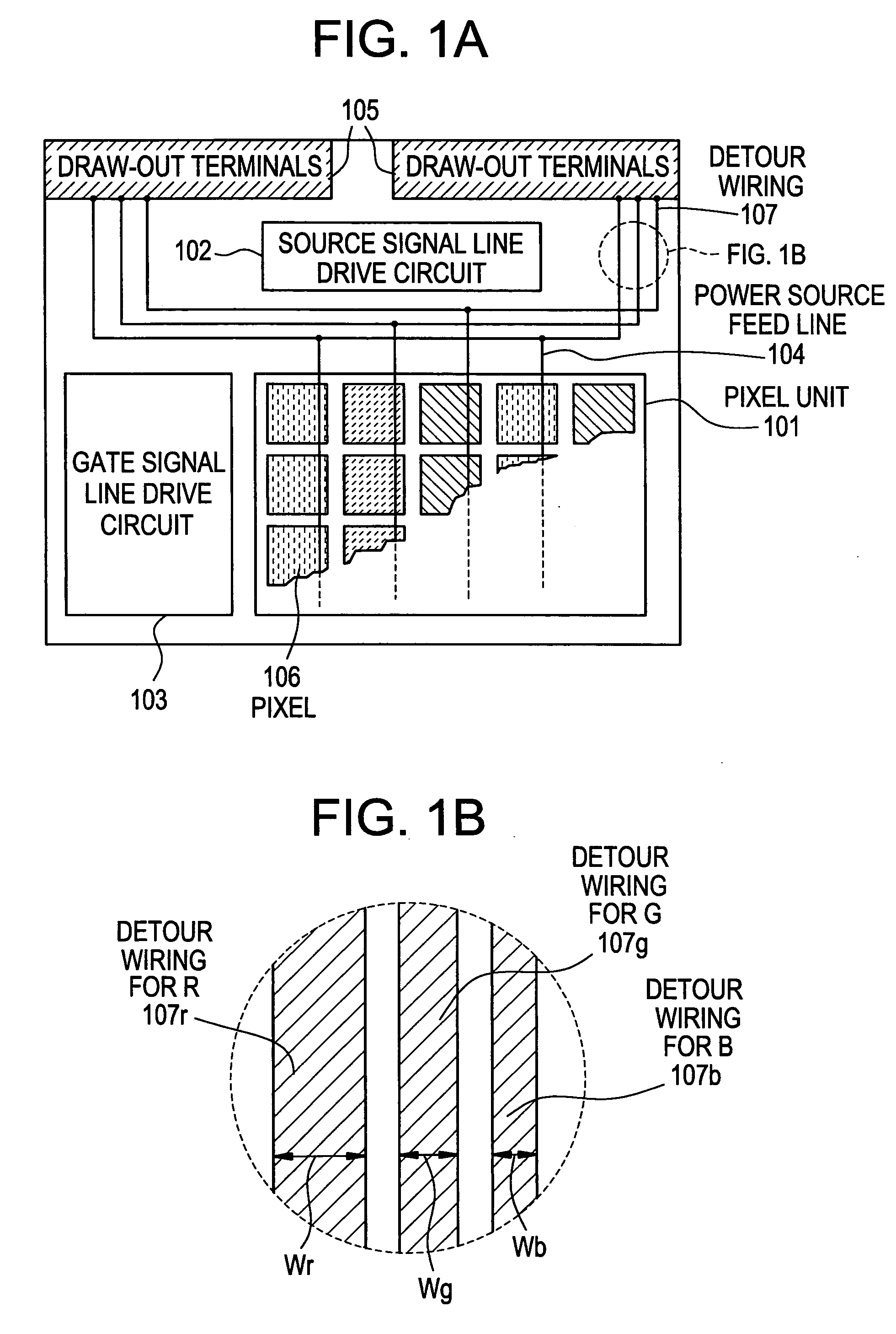
[0084] This embodiment deals with concrete numerical values of the widths of the detour wirings 107 shown in FIG. 1.

[0085] In this embodiment, the current densities through the organic EL materials of R, G and B are selected to be 7.5 mA / cm2, 3 mA / cm2 and 5 mA / cm2 so that the light-emitting brightnesses of the EL elements of R, G and B become 100 cd / m2, 100 cd / M2 and 50 cd / m2.

[0086] From the above current densities and in compliance with the formula 3, the ratio of widths of the power source feed lines for the pixels corresponding to R, G and B becomes as given by the formula 4,

Wr:Wg:Wb≅7.5:3:5   (4)

[0087] The balance in the light-emitting brightnesses of the pixels R, G, B can be maintained upon designing the widths of the detour wirings in accordance with the formula 4.

[0088] In this embodiment, the widths of the detour wirings corresponding to R, G and B need not satisfy the formula 4. The width of the detour wiring corresponding to R may be selected to be the greatest and t...


PUM


Abstract

A display device capable of displaying a picture of vivid colors maintaining a good balance of colors and a good balance of light-emitting brightnesses of the EL elements. The widths of the detour wirings supplying current to the power source feed lines are increased for those EL elements into which a current of a large density flows. This constitution decreases the wiring resistances of the detour wirings, decreases the potential drop through the detour wirings, and suppresses the amount of electric power consumed by the detour wirings.

Description

BACKGROUND OF THE INVENTION [0001] 1. Field of the Invention [0002] This invention relates to an EL (electroluminescence) display device (a light emitting device or a light emitting diode or OLED (Organic Light Emission Diode) formed by fabricating semiconductor elements (elements using a thin semiconductor film) on a substrate, and to an electronic device which uses the EL display device for a display unit thereof. The EL devices referred to in this specification include triplet-based light emission devices and / or singlet-based light emission devices, for example. [0003] 2. Related Art [0004] In recent years, technology for forming TFTs on a substrate has greatly advanced and study has been forwarded to apply the technology to the active matrix-type display devices. In particular, study has been vigorously forwarded concerning the active matrix-type EL display device using EL elements as spontaneously light-emitting elements among the active matrix type display devices. The EL disp...

Claims


Application Information

Patent Timeline
Patent Type & Authority Applications(United States)
IPC IPC(8): G09G3/32H01L27/32H05B44/00
CPCG09G3/3275H05B33/08G09G2300/0408G09G2300/0426G09G2300/0452G09G2300/0814G09G2300/0838G09G2300/0842G09G2300/0861G09G2310/0251G09G2310/0289G09G2310/061H01L27/3211H01L27/3276H01L27/3279H01L2227/323G09G3/3291Y02B20/30H05B44/00H10K59/35H10K59/1315H10K59/131H10K59/1201
Inventor YAMAZAKI, SHUNPEIKOYAMA, JUNINUKAI, KAZUTAKAOSAME, MITSUAKI
Owner SEMICON ENERGY LAB CO LTD
Why Eureka
Try Eureka