Data output control circuit
- Summary
- Abstract
- Description
- Claims
- Application Information
AI Technical Summary
Benefits of technology
Problems solved by technology
Method used
Image
Examples
Embodiment Construction
[0058] Hereinafter, a data output control circuit for use in a synchronous semiconductor memory device in accordance with the present invention will be described in detail referring to the accompanying drawings.
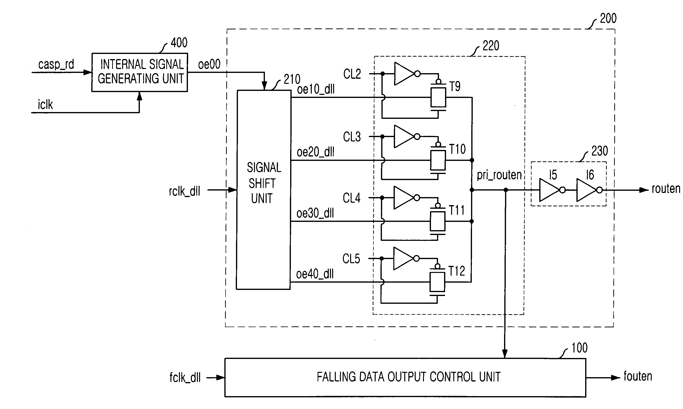
[0059]FIG. 5 is a block diagram showing a data output control circuit in accordance with a preferred embodiment of the present invention.
[0060] As shown, the data output control circuit includes an internal signal generating unit 400, a rising data output control unit 200 and a falling data output control unit 100.
[0061] The internal signal generating unit 400 receives a read command performing signal casp_rd and a clock signal iclk for generating an internal signal oe00 by synchronizing the read command performing signal casp_rd with the clock signal iclk.
[0062] The rising data output control unit 200 receives the internal signal oe00 and a delay locked rising edge clock signal rclk_dll for generating a rising data output enable signal routen in response to a CAS latency...
PUM
 Abstract
Description
Claims
Application Information


