Surface-emitting type semiconductor laser and method for manufacturing the same

a surface-emitting type, semiconductor laser technology, applied in semiconductor lasers, laser details, optical resonator shape and construction, etc., can solve the problems of difficult control of the polarization plane of a surface-emitting type semiconductor laser, difficult manufacturing method, and difficult stable manufactur

Inactive Publication Date: 2005-05-12
SEIKO EPSON CORP
View PDF10 Cites 32 Cited by
  • Summary
  • Abstract
  • Description
  • Claims
  • Application Information

AI Technical Summary

Benefits of technology

[0009] Exemplary aspects of the present invention provide surface-emitting type semiconductor lasers an

Problems solved by technology

However, the control of polarization planes of a surface-emitting type semiconductor laser is difficult because of the symmetry of its planar structure.
Therefore, when a surface-emitting type semiconductor laser is used for an optical system with a polarization dependence, instability of polarization planes causes n

Method used


Image

  • Surface-emitting type semiconductor laser and method for manufacturing the same
  • Surface-emitting type semiconductor laser and method for manufacturing the same
  • Surface-emitting type semiconductor laser and method for manufacturing the same

Examples


first exemplary embodiment

1. First Exemplary Embodiment

1-1. Device Structure

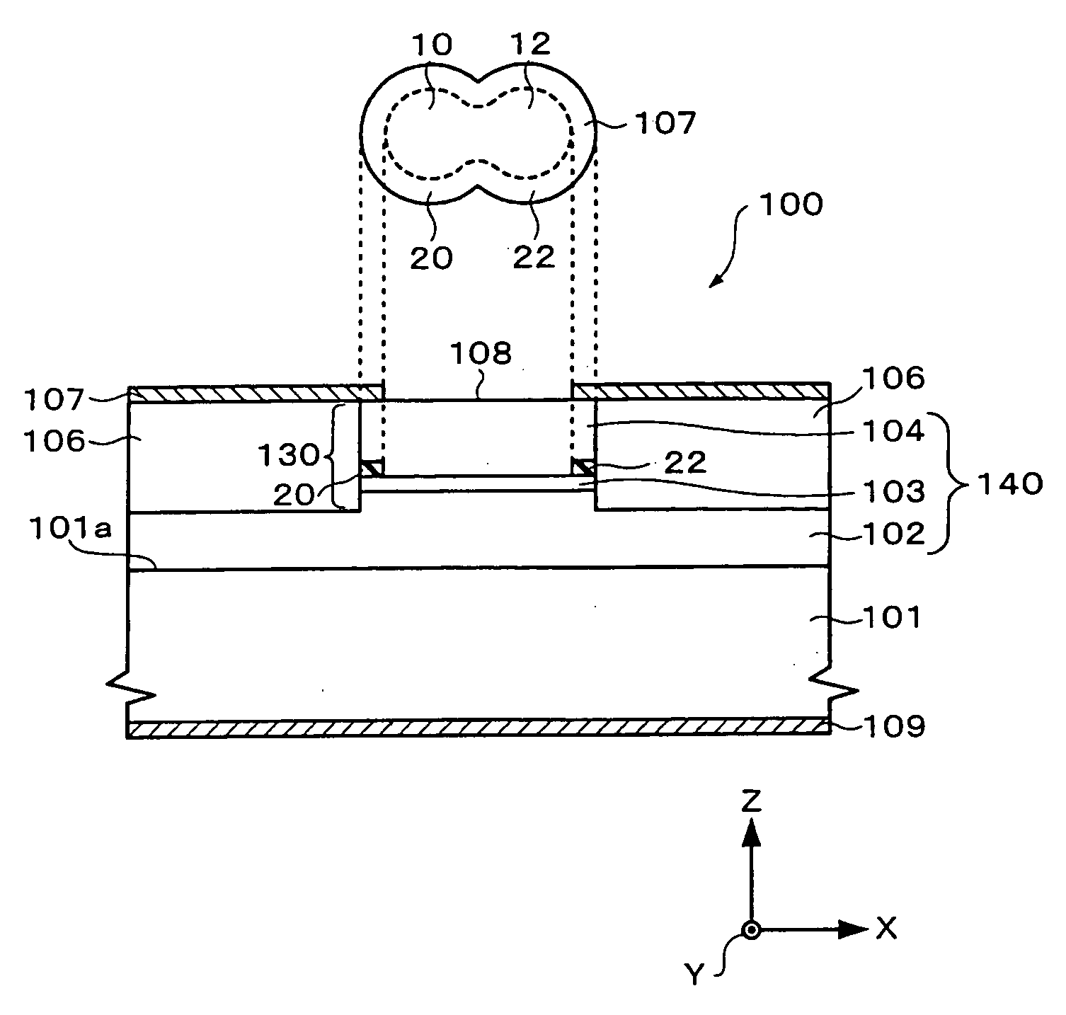
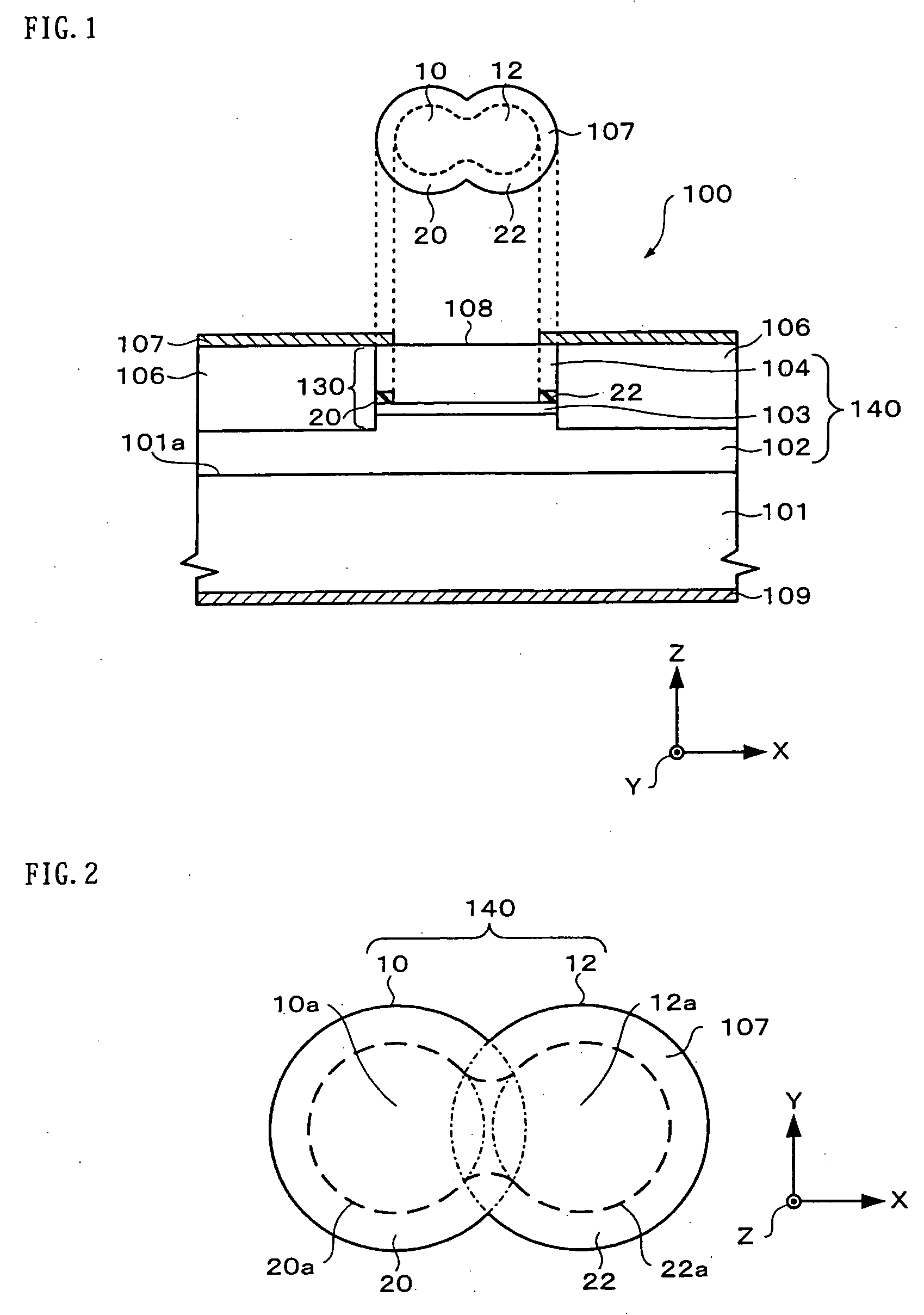
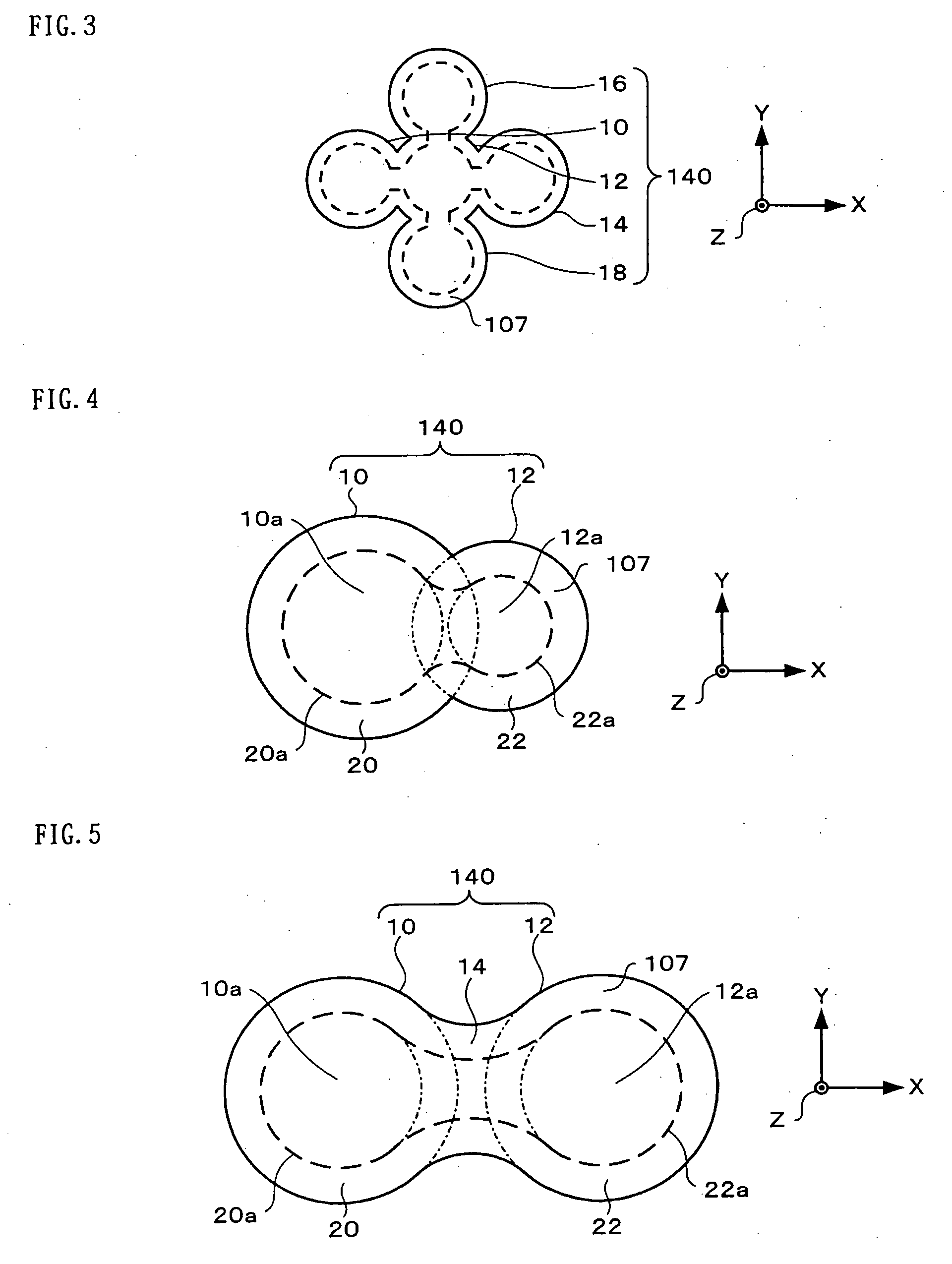
[0052]FIG. 1 is a schematic of a surface-emitting type semiconductor laser (hereinafter “surface emitting laser”) 100 in accordance with a first exemplary embodiment of the present invention. FIG. 2-FIG. 5 schematically show plan views of major portions of the surface-emitting laser 100 of the first exemplary embodiment.

[0053] The surface emitting laser 100 according to the present exemplary embodiment shown in FIG. 1 includes a semiconductor substrate (a GaAs substrate in the present exemplary embodiment) 101, a vertical resonator 140 formed on the semiconductor substrate 101, a first electrode 107 and a second electrode 109. The vertical resonator 140 includes a first mirror 102, an active layer 103, and a second mirror 104.

[0054] Next, components of the surface-emitting laser 100 are described below.

[0055] The vertical resonator 140 may be formed, for example, from the first mirror 102 that is a distributed reflection type mu...

second exemplary embodiment

2. Second Exemplary Embodiment

2-1 Device Structure

[0093]FIG. 11 is a schematic of a surface emitting laser 200 in accordance with a second exemplary embodiment of the present invention. FIG. 12-FIG. 14 are schematics show cross-sectional views of the surface-emitting laser 200 taken along planes A-A, lines B-B and lines C-C in FIG. 11, respectively. FIG. 15 is a schematic of major portions of the surface-emitting laser 200 in accordance with the second exemplary embodiment. The same reference numerals are appended to components that have substantially the same functions as those of the surface-emitting laser 100 in accordance with the first exemplary embodiment, and their detailed description is omitted.

[0094] As shown in FIG. 11-FIG. 14, the surface-emitting laser 200 of the present exemplary embodiment includes a semiconductor substrate (a GaAs substrate in the present exemplary embodiment) 101, a vertical resonator 140 formed on the semiconductor substrate 101, a first electro...


PUM


Abstract

To provide surface-emitting type semiconductor lasers and methods of manufacturing the same in which the polarization direction of laser light can be readily controlled, a surface-emitting type semiconductor laser includes a vertical resonator above a substrate. The vertical resonator includes a first mirror, an active layer and a second mirror disposed in this order from the substrate. The vertical resonator has a plurality of unit resonators. An emission region of each of the unit resonators has a diameter that oscillates in a single-mode.

Description

CROSS-REFERENCE TO RELATED APPLICATION [0001] The present application claims priority to Japanese Patent Application No. 2003-326296 filed Sep. 18, 2003 which is hereby expressly incorporated by reference herein in its entirety. BACKGROUND OF THE INVENTION [0002] 1. Field of Invention [0003] Exemplary aspects of present invention relate to surface-emitting type semiconductor lasers and methods for manufacturing the same. [0004] 2. Description of Related Art [0005] A surface emitting semiconductor laser is a semiconductor laser which emits laser light in a direction perpendicular to a semiconductor substrate. Since surface emitting type semiconductor lasers have excellent characteristics including, for example, easy handling, low threshold currents, etc., compared to related art edge emitting semiconductor lasers, application of surface emitting type semiconductor lasers to a variety of sensors and light sources for optical communications are expected. However, the control of polariz...

Claims


Application Information

Patent Timeline
IPC IPC(8): H01S5/183H01S5/42
CPCH01S5/18308H01S5/18311H01S5/18338H01S2301/176H01S5/18355H01S5/423H01S5/1835H01S5/18394H01S5/04256
Inventor NAKAYAMA, HITOSHIIDE, TSUGIOKANEKO, TSUYOSHI
Owner SEIKO EPSON CORP
Why Eureka
Try Eureka