Method of manufacturing an electronic device containing a carbon nanotube

a carbon nanotube and electronic device technology, applied in the manufacture of electric discharge tubes/lamps, instruments, electrode systems, etc., can solve the problems of difficult to obtain devices fully utilizing the characteristics of individual carbon nanotubes, the application of carbon nanotubes tending to get entangled with each other, and the inability to produce carbon nanotubes of the same structure. , to achieve the effect of good electron emission performance, good photoelectric performance and good photoelectric performan

Inactive Publication Date: 2005-12-27
CANON KK
View PDF15 Cites 36 Cited by
  • Summary
  • Abstract
  • Description
  • Claims
  • Application Information

AI Technical Summary

Benefits of technology

[0042]Another object of the invention is to provide a manufacturing method of carbon nanotube device in which the carbon nanotube binds to a conductive surface so that conduction is maintained therebetween, and the carbon nanotube has a high directivity.
[0043]Further, the invention has an object to provide an electron emission device giving a large quantity of electron emission and having a high performance.
[0053]According to the invention as described above, it is possible to control growth direction of the carbon nanotube by means of the wall. As a result, it is possible to provide an electron emitting device having excellent electron emitting properties, and a carbon nanotube device suitable for a probe of an STM or an AFM which gives a satisfactory image and has a high strength.
[0054]In the case where the wall comprises a layer containing alumina or silicon, it is possible to efficiently form a carbon nanotube device having a configuration in which a plurality of carbon nanotubes bind to the conductive surface, and binding sites of the individual carbon nanotubes are isolated from each other by the wall. The device of the invention, provided with carbon nanotubes whose growth directions are almost the same, and each of which have a uniform directivity isolated from each other at a high density, is suitably applicable for an electron emitting device or a probe such as an STM or an AFM.
[0055]When the conductive surface comprises a layer containing at least one material selected from the group consisting of titanium, zirconium, niobium, tantalum, molybdenum, copper and zinc, it is possible to easily form a carbon nanotube of the invention. More specifically, an alumina thin film having a narrow hole is formed through anodic oxidation also when forming the barrier by anodic oxidation of an aluminum thin film. The anodic oxidation carried out so that the bottom of the narrow hole serves as the electrode surface never damages the conductive surface, and as a result, it is possible to easily form a carbon nanotube binding conductively to the conductive surface.

Problems solved by technology

It is however not as yet possible to produce carbon nanotubes of the same structure.
Further, the carbon nanotubes in application tend to get entangled with each other in a complicated manner, and it is difficult to obtain devices fully utilizing characteristics of the individual carbon nanotubes.

Method used


Image

  • Method of manufacturing an electronic device containing a carbon nanotube
  • Method of manufacturing an electronic device containing a carbon nanotube
  • Method of manufacturing an electronic device containing a carbon nanotube

Examples


example 1

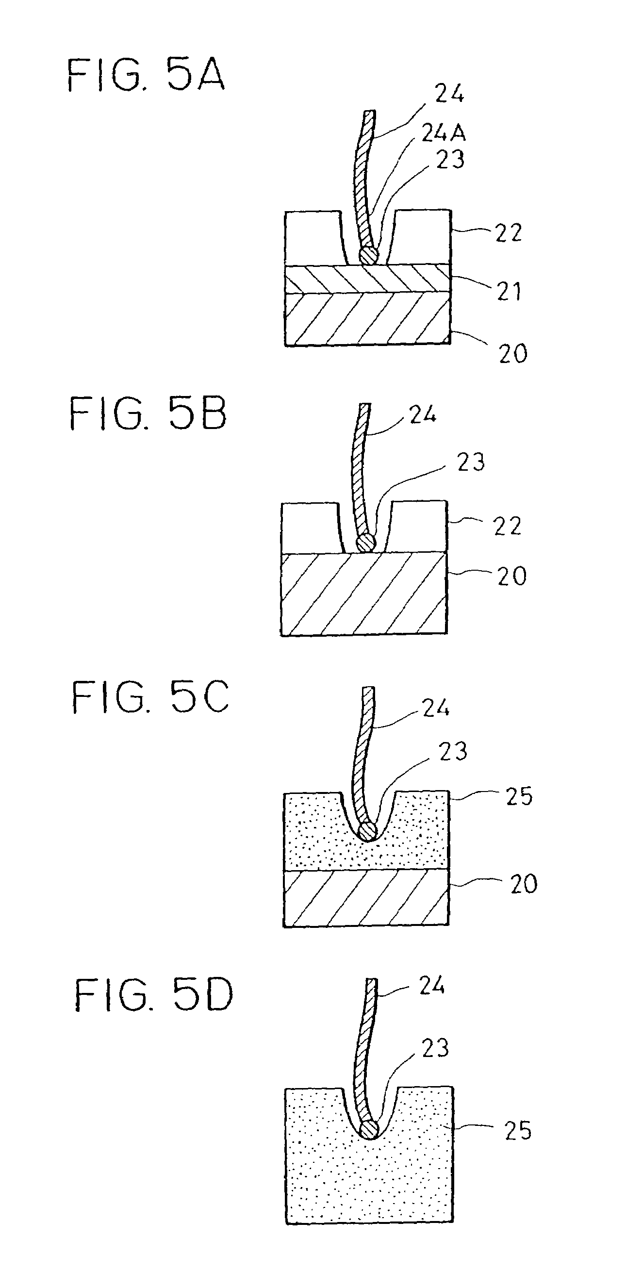
[0115](1) An Si wafer support having a clean surface was provided as a support. Ti was formed into a film having a thickness of 100 nm on the surface of the Si wafer by the sputtering process. The sputtering was carried out by applying RF power of 400 W and under Ar gas partial pressure of 5 mm Torr. After forming the Ti film, an Al film having a thickness of 1 μm was formed under the same conditions except for changing the target to Al in the same apparatus, thereby preparing a support 20 as shown in FIG. 8A.

[0116]A support having the layered structure as shown in FIG. 8A was prepared in the same manner as above except that the Ti thin film was changed to a Zr, Nb, Ta, Mo, Cu, Zn, Pd or Au thin film.

[0117]Each of the resultant supports was immersed in a 0.3 M oxalic acid solution, and then anodic oxidation of Al was carried out by using the support as an anode and Pt as a cathode and applying a voltage of 40 V while keeping a temperature of 17° C. As shown in FIG. 13, the beginning...

example 2

[0135]An example of the manufacturing method when the catalytic metal and the electrode film are the same will now be described.

[0136]As in Example 1, by the use of an Si wafer substrate cleaned as a support, a Co film having a thickness of 0.1 μm was formed on the support by the RF sputtering process. Then, in the same apparatus with the target changed to Al, and Al film was continuously formed into a thickness of 0.2 μm to form an Al / Co layered film. The sputtering conditions included an RF power of 400 W and an Ar atmosphere at 5 mTorr.

[0137]This support was immersed in a 0.3 M oxalic acid solution, and the Al film was anodically oxidized by using support as an anode and Pt as a cathode and impressing 40 V while keeping a temperature of 17° C. As a result of voltage impression, the Al surface was first rapidly oxidized, leading to a decrease in current value. After start of formation of narrow holes, the current value increased to a constant value. Upon the completion of oxidatio...

example 3

[0145]An example of carbon nanotube device in which the wall, the layer composing the conductive surface and the support are all prepared with Si will now be described with reference to the schematic process descriptive view shown in FIGS. 9A to 9C and the equipment schematic diagram shown in FIG. 7.

[0146]An ohmic contact was prepared by using a p-type substrate having a low resistance (several mm to several hundred mmΩcm) as a support, forming an Al film having a thickness of about 1 μm on the back of the p-type Si substrate and annealing at 400° C.

[0147]Then, anodization of the support was carried out with the support immersed in an aqueous solution containing 10% fluoric acid and 5% alcohol to serve as an anode and with Pt as a cathode. Al on the back was arranged so as not to come into contact with the fluoric acid solution, and an electrode was taken from the Al surface. Conditions were set to give a current value of several tens of mA / cm2 upon anodization. After the completion...


PUM

PropertyMeasurementUnit
diameteraaaaaaaaaa
diameteraaaaaaaaaa
temperatureaaaaaaaaaa

Abstract

A method of manufacturing an electronic device in which a substrate with a pair of electrodes is provided and a carbon nanotube is formed or arranged to electrically connect the electrodes.

Description

[0001]This application is a division of U.S. application Ser. No. 10 / 435,536, filed on May 12, 2003, now U.S. Pat. No. 6,720,728, which is a division of U.S. application Ser. No. 09 / 178,680, filed on Oct. 26, 1998, now U.S. Pat. No. 6,628,053 B1. The priority applications are incorporated herein by reference.BACKGROUND OF THE INVENTION[0002]1. Field of the Invention[0003]The present invention relates to a carbon nanotube device using a carbon nanotube and a manufacturing method thereof. More particularly, the invention relates to a carbon nanotube device applicable to a functional device such as a quantum-effect device, an electronic device, a micro-machine device or a bio-device etc. Further, the invention relates to a carbon nanotube device applicable to an electron source, an STM (scanning type tunnel microscope) probe, or an ATM (atomic force microscope) probe by the utilization of sharpness of the carbon nanotube, and a manufacturing method thereof.[0004]The invention relates a...

Claims


Application Information

Patent Timeline
Patent Type & Authority Patents(United States)
IPC IPC(8): C01B31/02D01F9/127G01B7/34G01N37/00G01Q30/12G01Q60/16G01Q60/38G01Q70/12G01Q70/14G01Q70/16G01Q90/00H01B1/04H01J1/304H01J9/02H01L21/00H01L29/06H01L49/00
CPCB82Y15/00B82Y30/00B82Y35/00D01F9/127G01Q60/16G01Q60/38G01Q70/12H01J1/14H01J1/30H01J1/304H01J9/025B82Y10/00H01J2201/30469Y10S977/932Y10S977/939
Inventor DEN, TOHRUIWASAKI, TATSUYA
Owner CANON KK
Why Eureka
Try Eureka