

Packaging device for matrix-arrayed semiconductor light-emitting elements of high power and high directivity
- Summary
- Abstract
- Description
- Claims
- Application Information
AI Technical Summary
Benefits of technology
Problems solved by technology
Method used
Image

Examples
Embodiment Construction
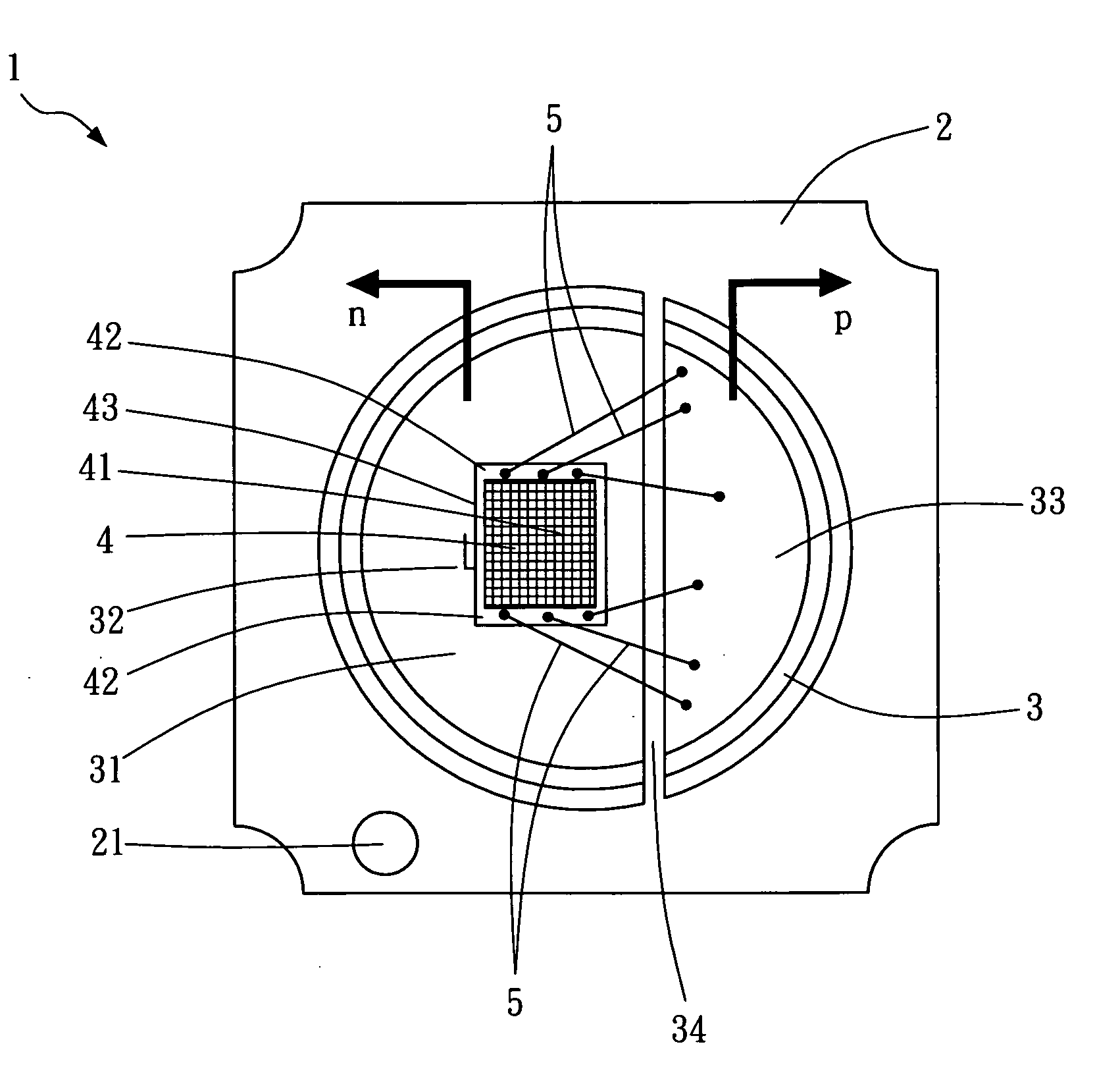
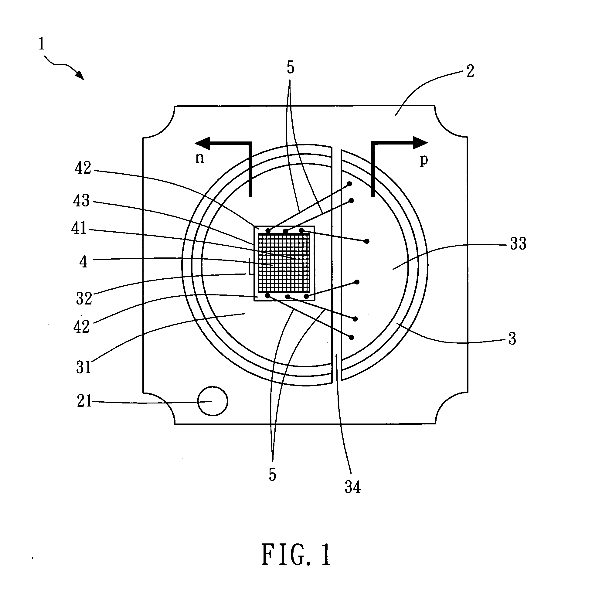
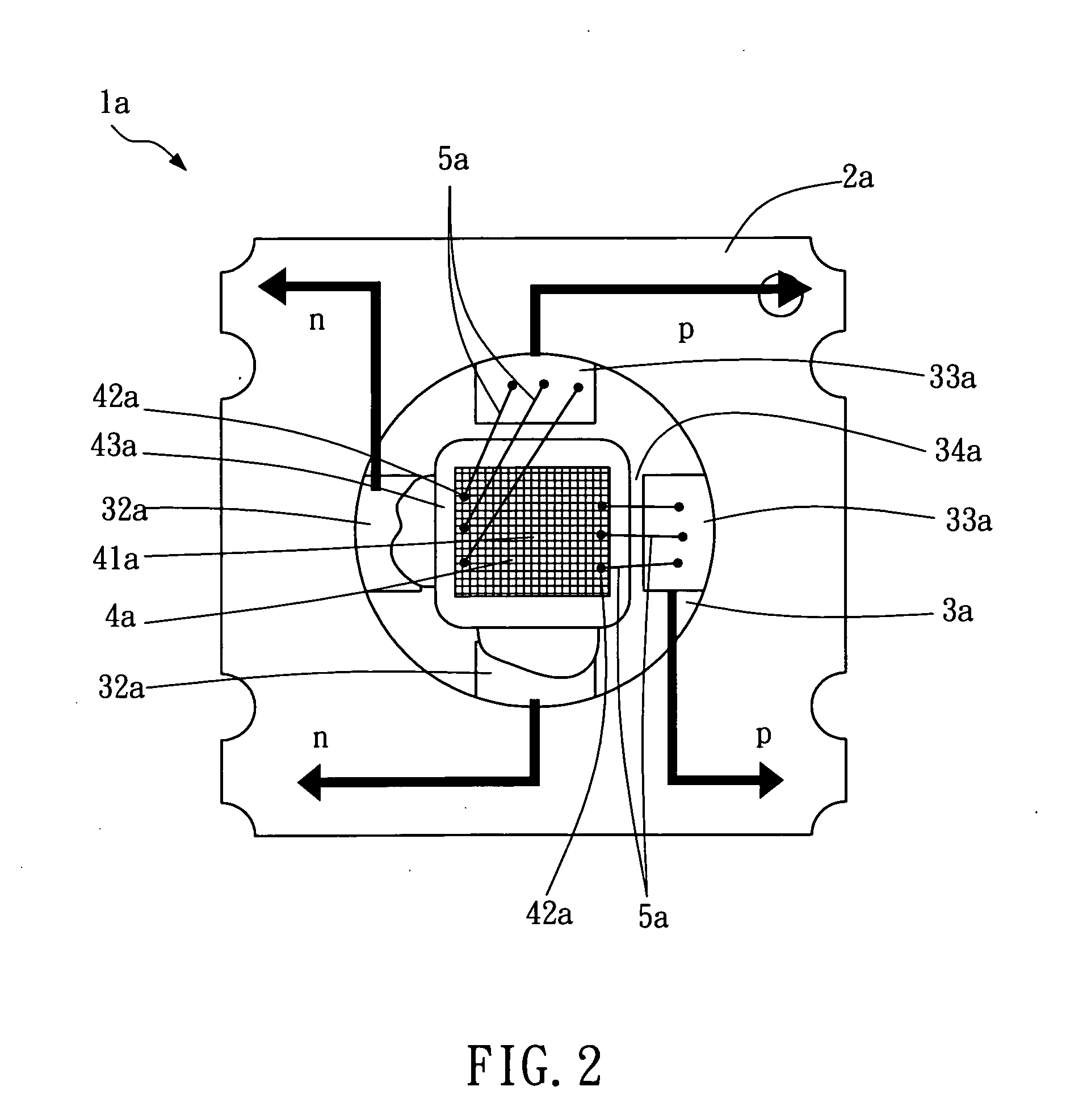
[0021]FIG. 1 is a top view of a first embodiment of the packaging device for matrix-arrayed semiconductor light-emitting elements of high power and high directivity according to the present invention. In the first embodiment, the packaging device 1 comprises a circuit board 2, a metal substrate 3, an array chip 4, and a plurality of metal wires 5.
[0022]The circuit board 2 is used to carry the metal substrate 3, and leads, stems, pins or terminals (not shown in FIG. 1) capable for electrical connection to external printed circuit boards (not shown) are disposed below or laterally to the circuit board 2, wherein at least one hole 21 is disposed on the circuit board 2. In this embodiment, the circuit board 2 may preferably be an LTCC (Low Temperature Co-fired) substrate, an HTCC (High Temperature Co-fired Ceramic) substrate, or a plastic substrate.
[0023]The metal substrate 3 adhered to the circuit board 2 has a supporting surface 31 for supporting elements such as the array chip 4 and ...
PUM
 Abstract
Description
Claims
Application Information