Methodology to optimize hierarchical clock skew by clock delay compensation

a hierarchical clock and delay compensation technology, applied in the direction of generating/distributing signals, instruments, program control, etc., can solve the problems of excessive run time and memory load, inability to completely balance the number of buffers,

Inactive Publication Date: 2005-05-12
TAIWAN SEMICON MFG CO LTD
View PDF9 Cites 46 Cited by
  • Summary
  • Abstract
  • Description
  • Claims
  • Application Information

AI Technical Summary

Problems solved by technology

It is not possible to either totally balance the number of buffers or the amount of wiring segment used in creating the clock distribution.
Too few segments yields sub-par solutions, but too many segments can lead to excessive run times and memory loads.

Method used


Image

  • Methodology to optimize hierarchical clock skew by clock delay compensation
  • Methodology to optimize hierarchical clock skew by clock delay compensation
  • Methodology to optimize hierarchical clock skew by clock delay compensation

Examples


Embodiment Construction

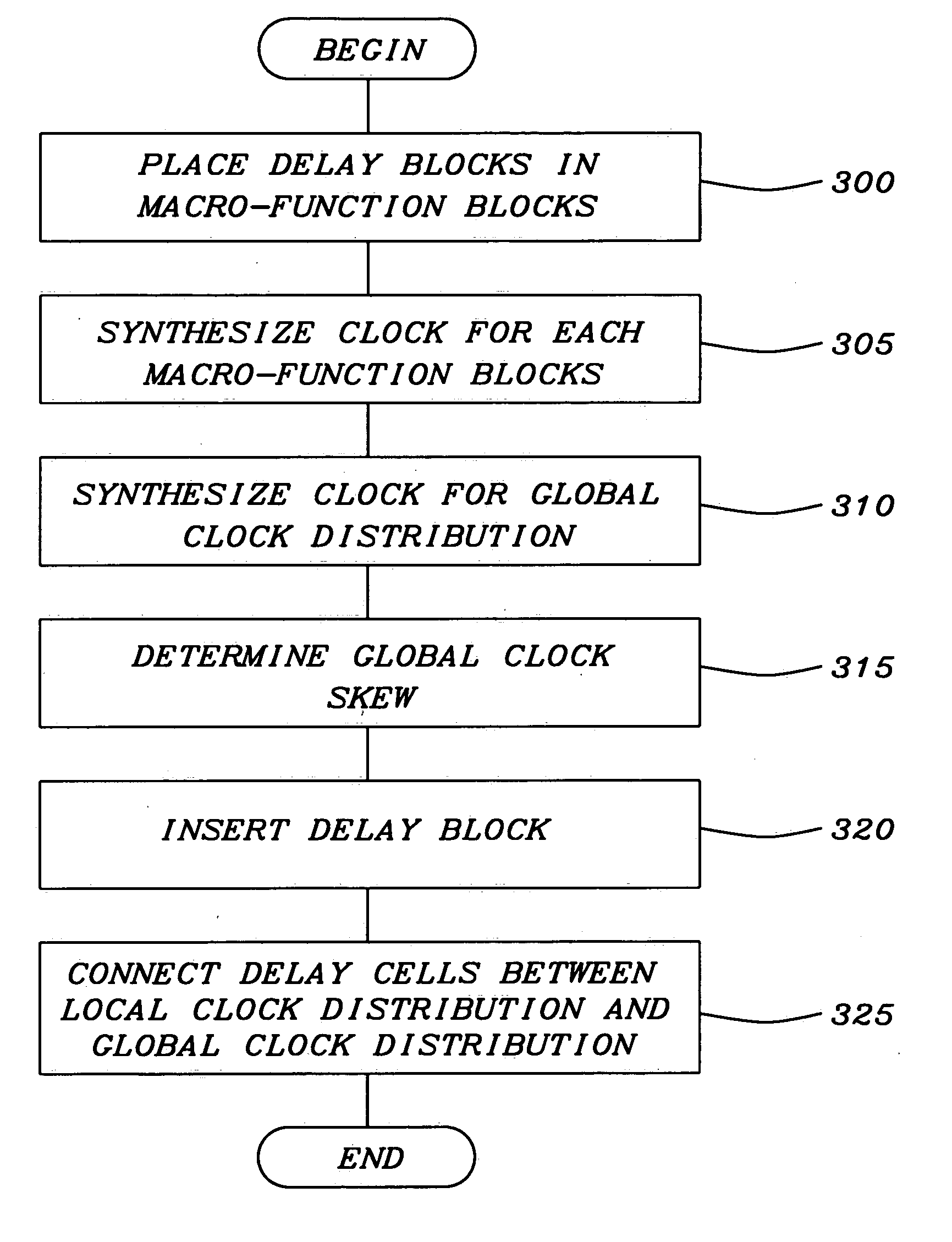
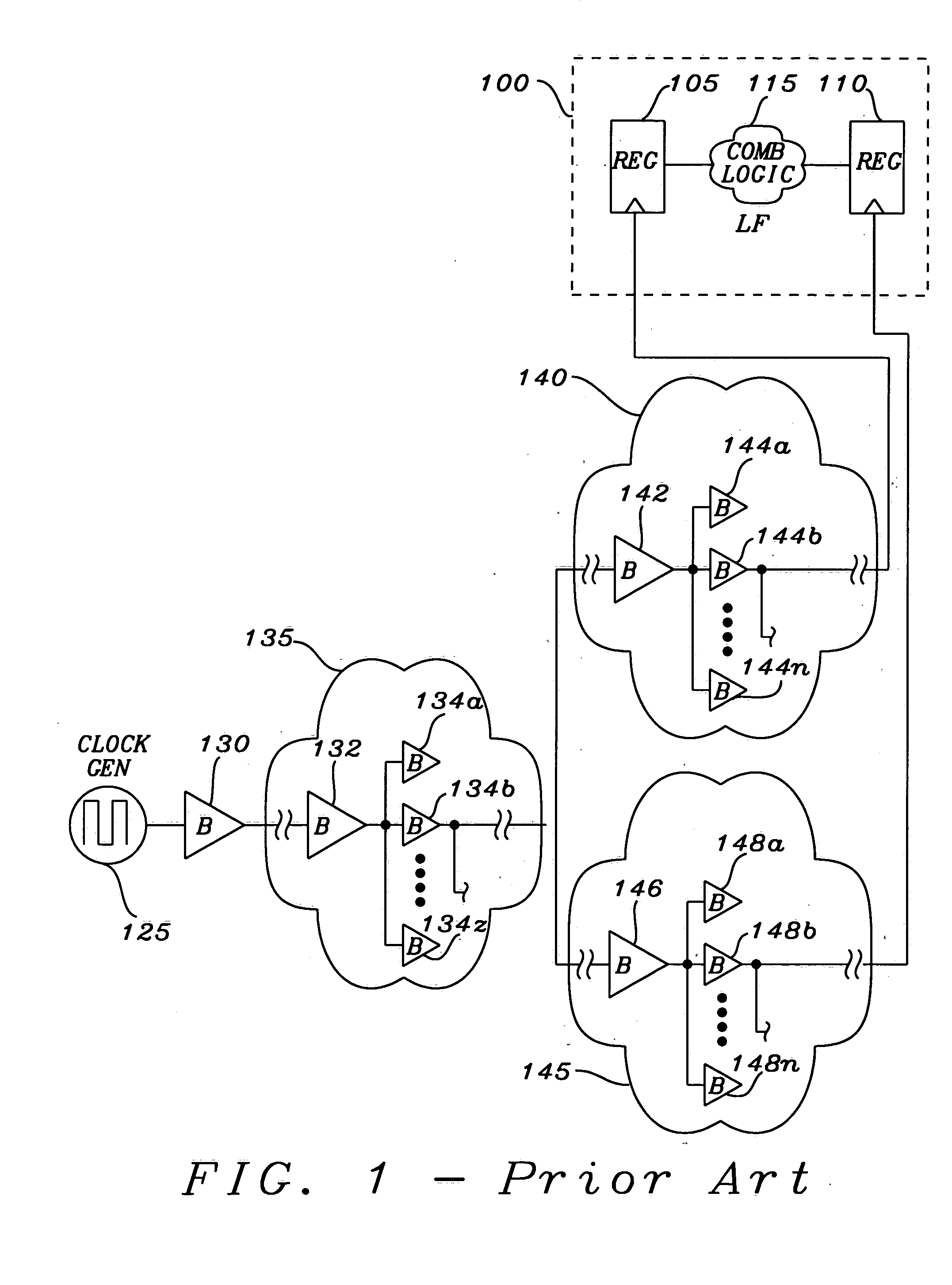
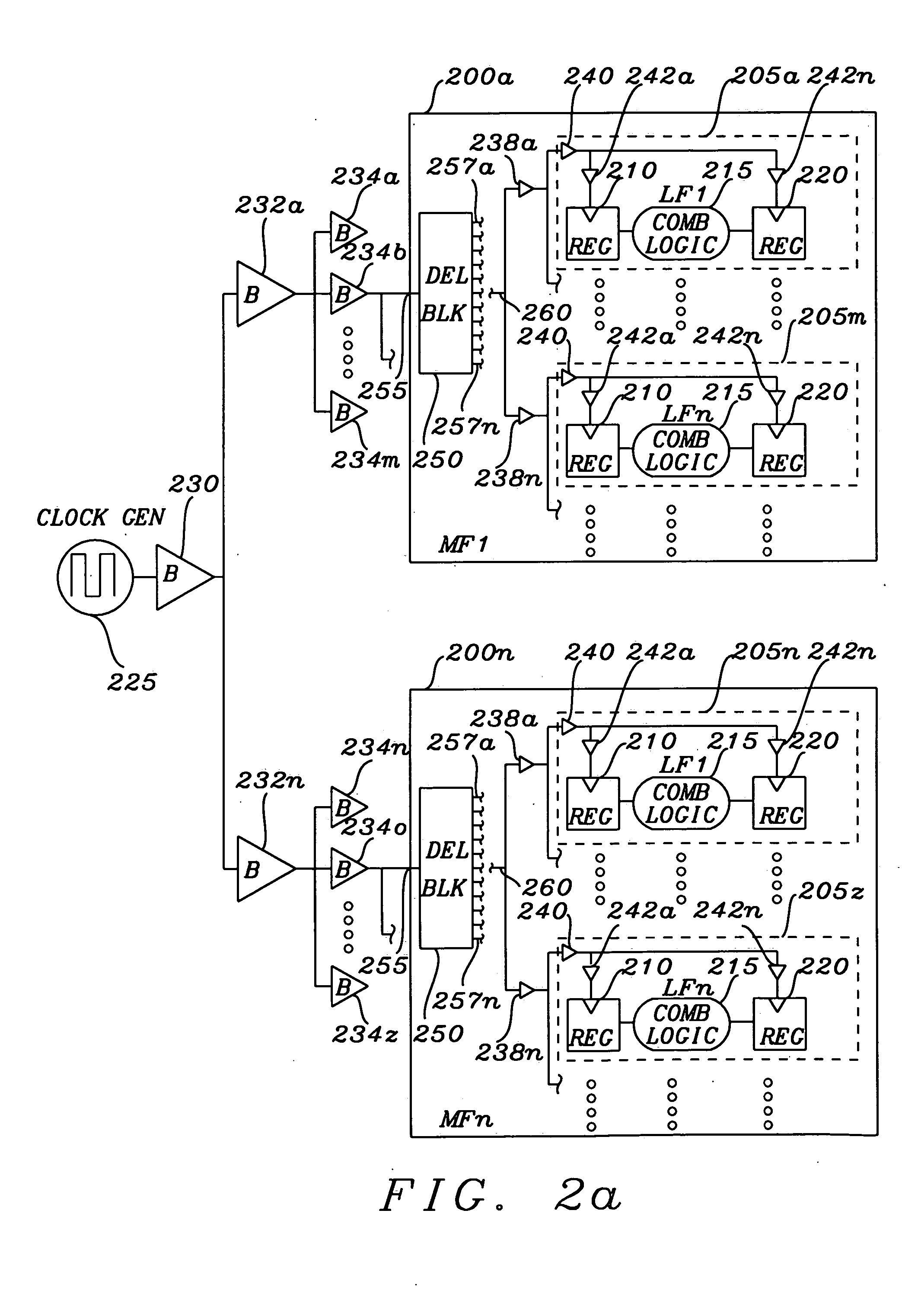
[0032] In an integrated circuit of this invention, the clock distribution circuit has a network of inter-functional buffer circuits connected to distribute a clock timing signal from a clock generator to each macro-function circuit of the integrated circuit device. Within each macro-function circuit, a network of intra-functional buffer circuits is connected to distribute the clock timing signal to the register circuits of each synchronous functional circuit. An adjustable delay block is placed at the boundary of each of the macro-function circuits. During the physical design layout of the integrated circuit device, the intra-functional clock distribution network is designed. Once the global functions have been arranged on the semiconductor substrate and the intra-functional clock distribution network designed, the inter-functional clock distribution network is constructed. The differences of the delays for branch of the inter-functional distribution network is calculated to determi...


PUM


Abstract

A method for synthesizing a clock distribution system within an integrated circuit for compensating for clock skew within a global or top level clock distribution network begins with allocating at least one delaying circuit within each of functional circuits of the integrated circuit. An intra-functional clock distribution network is fabricated within each of the functional circuits. Once the intra-functional clock distribution network is fabricated, an inter-functional clock distribution network is constructed between each of the functional circuits. A clock skew for the inter-functional clock distribution network is determined. The clock skew is then compensated by inserting the delaying circuit at a terminal of the inter-function clock distribution network where each of the functional circuits is connected to the inter-functional clock distribution network.

Description

BACKGROUND OF THE INVENTION [0001] 1. Field of the Invention [0002] The present invention relates generally to methods and apparatus for the design, partition, and placement of microelectronic integrated circuits. More specifically, the present invention is related methods and apparatus for the design and construction of a hierarchical clock distribution system within microelectronic integrated circuits. Even more particularly the present invention relates to methods and apparatus for compensating for clock skew within the clock distribution system between functional circuit blocks of the integrated circuits. [0003] 2. Description of Related Art [0004] Electronic Design Automation (EDA) tools and methods facilitate the design, partition, and placement of microelectronic integrated circuits on a semiconductor substrate. Generally transistors are formed into primitive circuits that perform digital logic functions such as AND, OR, NAND, NOR, etc. The primitive circuits are then organiz...

Claims


Application Information

Patent Timeline
Patent Type & Authority Applications(United States)
IPC IPC(8): G06F1/10G06F9/45G06F17/50
CPCG06F17/5045G06F1/10G06F30/30
Inventor HOU, CLIFFCHENG, CHIA-LINLU, LEE-CHUNG
Owner TAIWAN SEMICON MFG CO LTD
Why Eureka
Try Eureka