
Plasma display panel and method of manufacturing the plasma display panel

a technology of plasma display panel and display panel, which is applied in the manufacture of electrode systems, electric discharge tubes/lamps, and gas discharge sealing. it can solve the problems of increasing the cost of fabricating the bus electrode in the non-display area that is electrically connected to the external terminal, increasing the cost of bus electrodes, and increasing the risk of developing solutions

Inactive Publication Date: 2005-05-19
SAMSUNG SDI CO LTD
View PDF17 Cites 12 Cited by
  • Summary
  • Abstract
  • Description
  • Claims
  • Application Information

AI Technical Summary

Benefits of technology

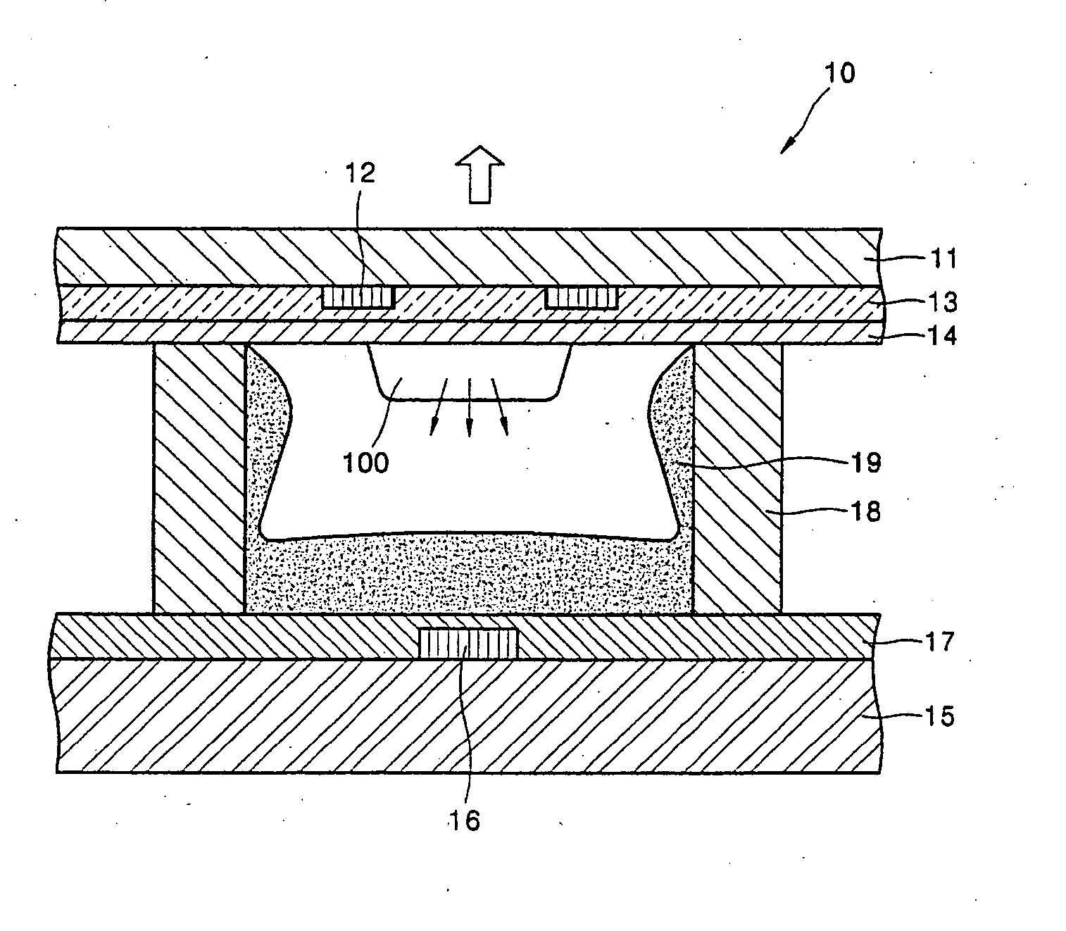
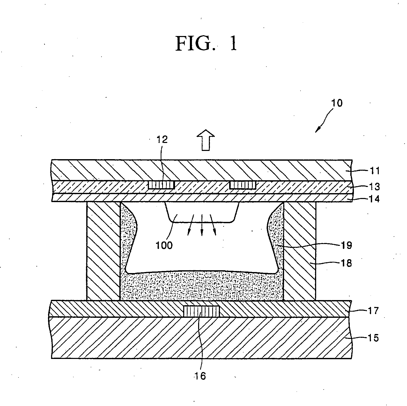
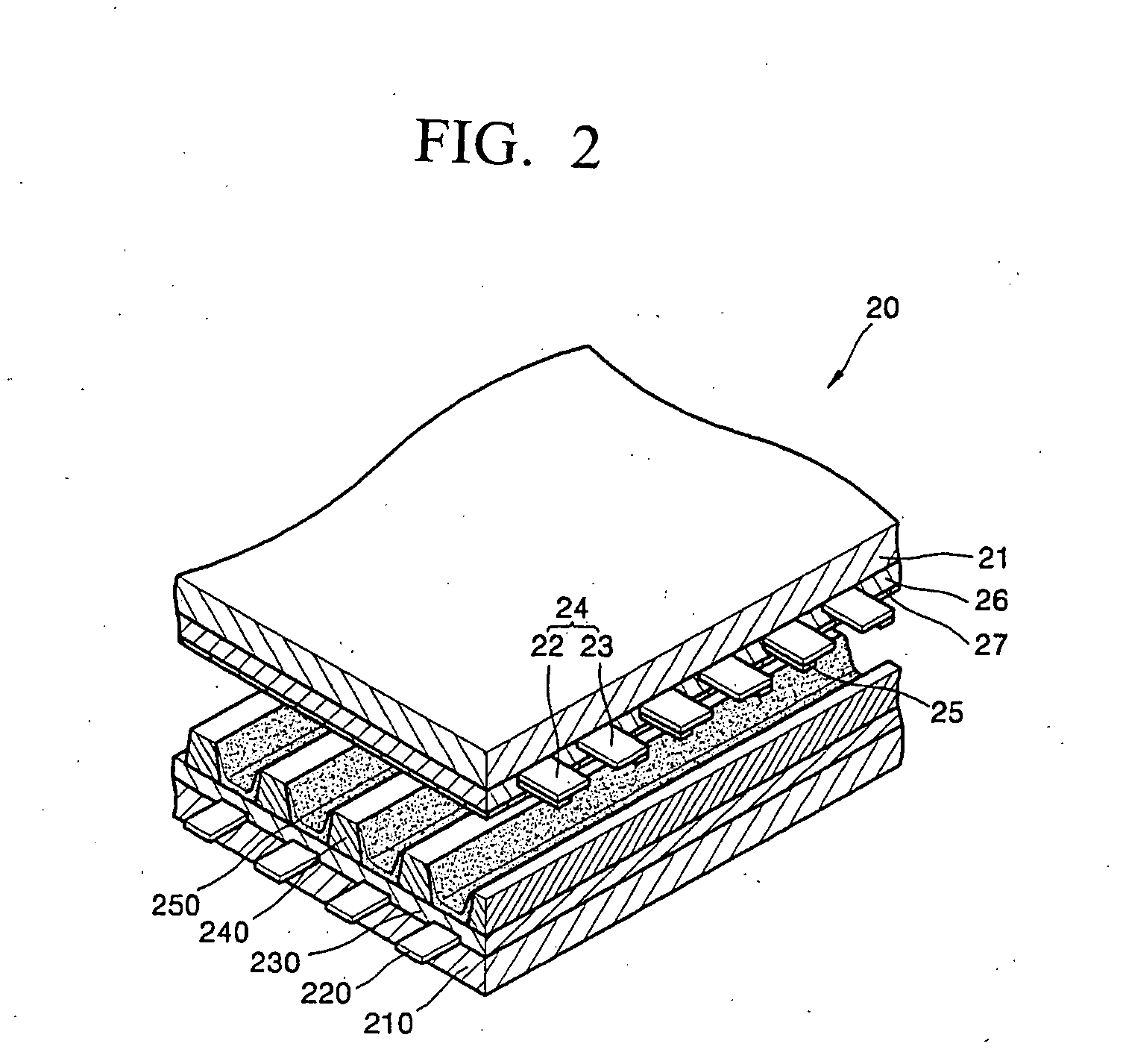
[0021] The present invention provides a Plasma Display Panel (PDP) having improved contrast and brightness by forming a bus electrode to have different respective structures of electrodes on a display area and on a non-display area of a substrate, and a method of fabricating the PDP.

Problems solved by technology

However, the bus electrode formed on the PDP has the following problems.
When a raw material for forming the bus electrode is printed and developed, the first bus electrode is more vulnerable to a developing solution than the second bus electrode.
If the undercut portion is large, it may cause a short.
However, a center portion of the bus electrode tends to contract downward.
In addition, since the thickness of the bus electrode patterned on the front substrate is constant on the display area and on the non-display area, the cost of fabricating the bus electrode on the non-display area that is electrically connected to the external terminal increase greatly when the size of the PDP becomes larger.

Method used


Image

  • Plasma display panel and method of manufacturing the plasma display panel
  • Plasma display panel and method of manufacturing the plasma display panel
  • Plasma display panel and method of manufacturing the plasma display panel

Examples


first embodiment

[0092]FIGS. 9 and 10 are views of the bus electrode according to the present invention.

[0093] Referring to FIG. 9, the bus electrode includes the display unit bus electrode 91 formed on the display area D, and non-display unit bus electrodes 92 formed on the non-display areas E and F.

[0094] The display unit bus electrode 91 includes a first bus stripe electrode 93. The first bus electrode 93 contacts the surface of the front substrate 71 (refer to FIG. 7).

[0095] The first bus electrode 93 functions as a shielding layer for improving a contrast of the PDP, and is a conductive or a nonconductive black layer. It is desirable that the first bus electrode 93 is formed of a material in which a black material such as Co, Cr, or Ru is mixed with a frit powder. The first bus electrode 93 is formed only on the display area D, and a thickness of the first bus electrode 93 is about 1˜2 μm.

[0096] A second bus electrode 94 is formed on the first bus electrode 93. The second bus electrode 94 is...

third embodiment

[0120]FIG. 14 is a view of a bus electrode according to the present invention.

[0121] Referring to FIG. 14, the bus electrode includes a display unit bus electrode 140 and a non-display unit bus electrode 150 that is electrically connected to the display unit bus electrode 140.

[0122] The display unit bus electrode 140 has the dual-layered structure including a black first bus electrode 141 that is coated on the front substrate 71, and a white second bus electrode 142 that is coated on the upper surface of the first bus electrode 141.

[0123] The non-display unit bus electrode 150 is coated on the front substrate 71, and has the single-layered structure that is electrically connected to at least one electrode in the display unit bus electrode 140.

[0124] Since the non-display unit bus electrode 150 is thinner than the display unit bus electrode 140, a short can occur. In order to prevent the short from occurring, it is desirable that a width W4 of the non-display unit bus electrode 15...

fourth embodiment

[0125]FIGS. 15 and 16 are views of a bus electrode according to the present invention.

[0126] Referring to FIGS. 15 and 16, the bus electrode includes a display unit bus electrode 160 formed on the display area and a non-display unit bus electrode 170 formed on the non-display area.

[0127] The display unit bus electrode 160 includes a first bus electrode 161 formed on the front substrate 71, and a second bus electrode 162 formed on the first bus electrode 161. The first and second bus electrodes 161 and 162 are white and are formed of same material.

[0128] On the contrary, the non-display unit bus electrode 170 is electrically connected to at least one electrode of the display unit bus electrode 160, and is a single layer formed on the front substrate 71. The non-display unit bus electrode 170 is also white.

[0129] That is, the black bus electrode that functions as the shielding layer is not included in the display unit bus electrode 160, as well as in the non-display unit bus electr...


PUM


Abstract

A Plasma Display Panel (PDP) includes: a front substrate, a common electrode and a scan electrode arranged on a lower surface of the front substrate, a bus electrode electrically connected to the common electrode and the scan electrode, a front dielectric layer covering the common electrode, the scan electrode, and the bus electrode, a rear substrate facing the front substrate, an address electrode arranged on an upper surface of the rear substrate to cross the bus electrode, a barrier rib arranged between the front and rear substrates, and a phosphor layer arranged on a discharge space defined by the barrier rib. The bus electrode includes a display unit bus electrode arranged on a display area that displays pixels, and a non-display unit bus electrode arranged on a non-display area electrically connected to the display unit bus electrode and connected to an external terminal. The display unit bus electrode and the non-display unit bus electrode have different structures. The non-display unit bus electrode arranged on the non-display area is a single-layered structure while the display unit bus electrode arranged on the display area is a double-layered structure.

Description

CLAIM OF PRIORITY [0001] This application makes reference to, incorporates the same herein, and claims all benefits accruing under 35 U.S.C. §119 from an application for PLASMA DISPLAY AND METHOD OF FABRICATING THE SAME earlier filed in the Korean Intellectual Property Office on 17 Nov. 2003 and there duly assigned Serial No. 2003-81112. BACKGROUND OF THE INVENTION [0002] 1. Field of the Invention [0003] The present invention relates to a plasma display panel, and more particularly, to a plasma display panel having bus electrodes of different respective structures on a display area and a non-display area, and a method of manufacturing the plasma display panel. [0004] 2. Description of the Related Art [0005] A Plasma Display Panel (PDP) is a flat display device that displays letters or graphics using light emitted by plasma generated in a gas discharge process. The PDP can be either a Direct Current (DC) PDP, in which an electrode for applying voltages from the outside is directly ex...

Claims


Application Information

Patent Timeline
Patent Type & Authority Applications(United States)
IPC IPC(8): H01J11/22H01J11/24H01J11/34H01J11/46H01J9/02H01J11/48
CPCH01J11/12H01J2211/245H01J11/46H01J11/22H01J9/02
Inventor HONG, CHONG-GIKANG, TAE-KYOUNG
Owner SAMSUNG SDI CO LTD
Learn More