Solid-state imaging device

a solid-state imaging and imaging device technology, applied in the direction of color television, television system, radio control device, etc., can solve the problems of slow signal output rise, dark defects, linearity worsening,

Inactive Publication Date: 2005-05-26
SEIKO EPSON CORP
View PDF10 Cites 4 Cited by
  • Summary
  • Abstract
  • Description
  • Claims
  • Application Information

AI Technical Summary

Benefits of technology

[0020] With this configuration, supposing, for example, that the carrier pocket is provided in a ring shape with a roughly constant width under the ring gate, and near the circumference in the major-axis direction of the oval source region and, further, near the circumference of the ring gate in the minor-axis direction of the oval source region by fo

Problems solved by technology

Therefore, low light intensity results in the slow rising of signal outputs, worsening linearity (see line h in FIG. 9), and thereby causing dark defects.
As described above, local non-uniformi

Method used


Image

  • Solid-state imaging device
  • Solid-state imaging device
  • Solid-state imaging device

Examples


first embodiment

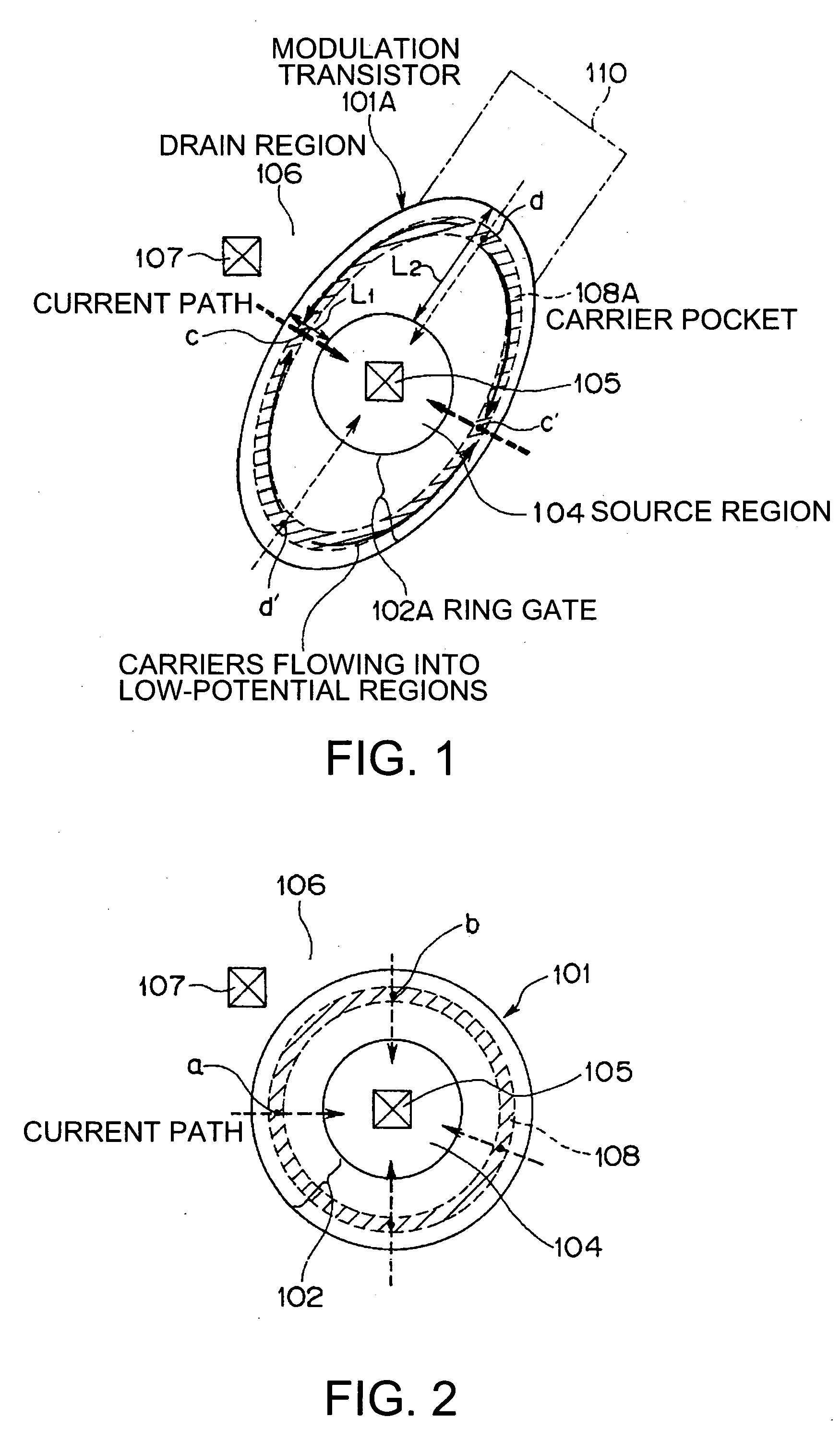
[0034]FIG. 1 is a schematic top-view drawing of a modulation transistor in a solid-state imaging device of a first embodiment of the present invention. FIG. 2 is a schematic view of a conventional modulation transistor (along line A-A′ shown in FIG. 6, the photodiode is not illustrated). FIG. 3 is a graph for comparing surface potential between the modulation transistor according to the present invention and the conventional modulation transistor. For parts that are the same as those shown in FIG. 5, the same numbers are assigned for explanation. In FIG. 1, a modulation transistor 101A according to the first embodiment of the present invention configures a sensor cell together with a photodiode (shown by a two-dot chain line 110) which receives incident light. A ring gate 102A has an oval contour (perimeter shape). The source region 104 is formed in a round shape at the center of the ring gate 102A. A carrier pocket 108A is formed in a ring-shaped narrow band with a roughly constant...

second embodiment

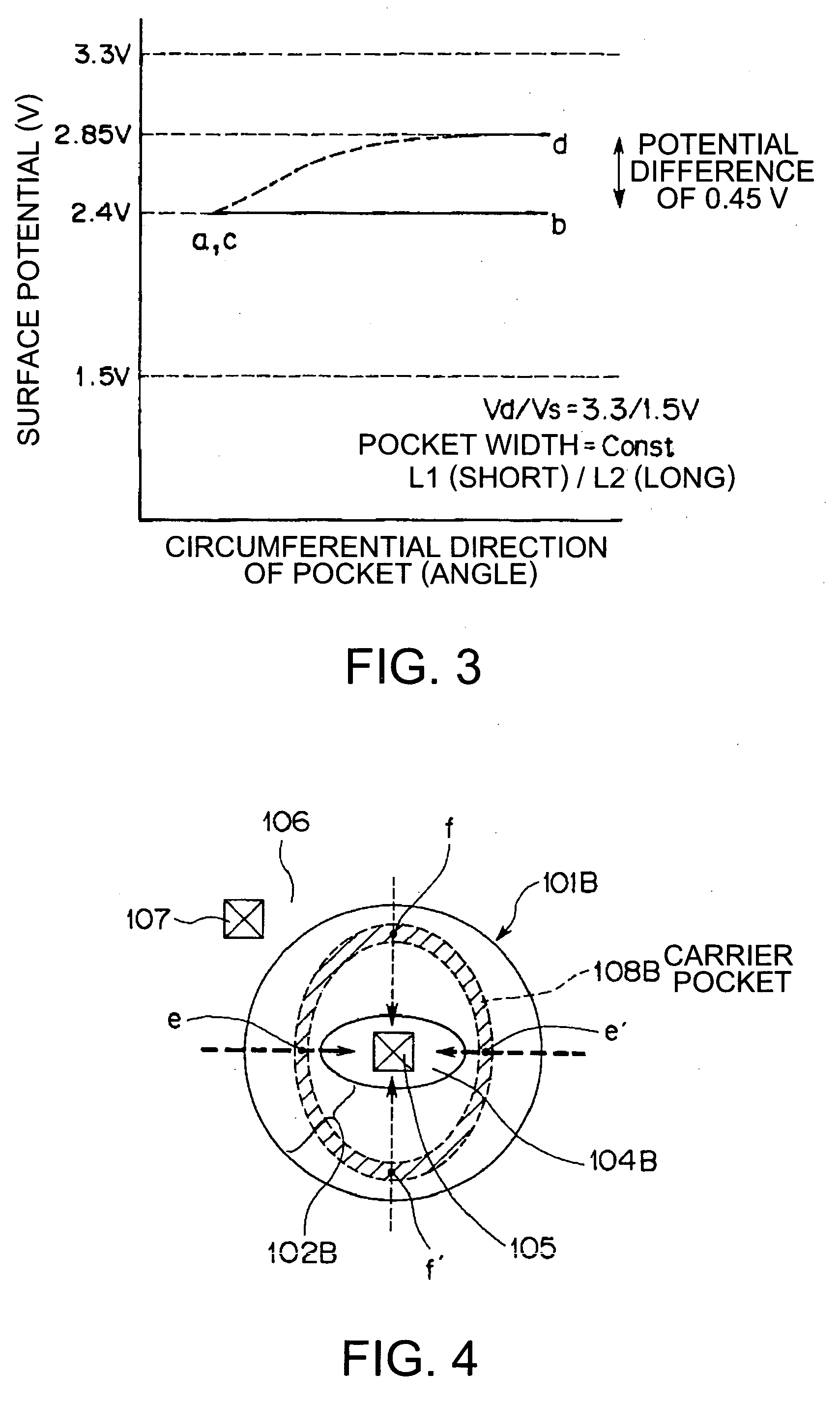
[0044]FIG. 4 is a schematic top-view drawing of a modulation transistor in a solid-state imaging device of a second embodiment of the present invention. In the actual configuration of the sensor cells, there is a photodiode adjacent to the modulation transistor, which is omitted here.

[0045] In FIG. 4, a modulation transistor 101B according to the second embodiment of the present invention configures a sensor cell together with a photodiode (not illustrated) which receives incident light. A ring gate 102B has a round contour (perimeter shape). A source region 104B is formed in an oval shape at the center of the ring gate 102B. A carrier pocket 108B is provided in an approximate oval shape with a roughly constant width under the ring gate 102B and near the circumference in the major-axis direction of the oval source region 104B and, further, near the circumference of the ring gate 102B in the minor-axis direction of the oval source region 104B. The source contact 105 is located at th...


PUM


Abstract

A solid-state imaging device is provided which has preferable linearity of signal outputs according to light intensities and does not cause dark defects even at a low light intensity. The solid-state imaging device comprises: a ring gate having a non-uniform width; a source region formed inside the ring gate; a drain region formed surrounding a circumference of the ring gate; and a carrier pocket formed under the ring gate, wherein a region where (X divided by Y) is the smallest substantially coincides with a region where Z is the shortest; X is a pocket-to-source distance; Y is a pocket-to-drain distance; and Z is a source-to-drain distance.

Description

RELATED APPLICATIONS [0001] This application claims priority to Japanese Patent Application No. 2003-395615 filed Nov. 26, 2003 which is hereby expressly incorporated by reference herein in its entirety. BACKGROUND [0002] 1. Field of the Invention [0003] The present invention relates to a solid-state imaging device providing high image quality and low power consumption and, especially, a solid-state imaging device, having a ring-shaped gate, which can obtain signal outputs by modulating threshold voltages (Vth) in accordance with subject light. [0004] 2. Related Art [0005] As solid-state imaging devices to be built in cellular phones, etc., there are two types of image sensors: charge-coupled device (CCD) image sensors; and CMOS image sensors. CCD image sensors are superior in image quality, while CMOS image sensors consume lower power and process cost. In recent years, proposals have been made for MOS imaging devices employing threshold voltage modulation which provides both high i...

Claims


Application Information

Patent Timeline
IPC IPC(8): H01L31/113H01L27/146H04N5/335H04N5/355H04N5/369H04N5/374
CPCH01L27/14609H01L27/14603
Inventor KUWAZAWA, KAZUNOBU
Owner SEIKO EPSON CORP
Why Eureka
Try Eureka