Structure and method to fabricate finfet devices

Inactive Publication Date: 2005-05-26
GLOBALFOUNDRIES INC
View PDF18 Cites 8 Cited by
  • Summary
  • Abstract
  • Description
  • Claims
  • Application Information

AI Technical Summary

Benefits of technology

[0011] It is another object of the present invention to provide a method for fabricating a FinFET that minimizes or eliminates the negative effects of over-etching.
[0012] It is still another object of the present invention to provide a method for fabricating a FinFET that uses a self-limitin

Problems solved by technology

Current FinFET process technology suffers from certain drawbacks.
One significant drawback stems from the sacrificial oxidation and pre-gate oxide clean processes.
Hence, substantially thin fins, which are commonly used for gate-length scaling, can be under

Method used


Image

  • Structure and method to fabricate finfet devices
  • Structure and method to fabricate finfet devices
  • Structure and method to fabricate finfet devices

Examples


Example

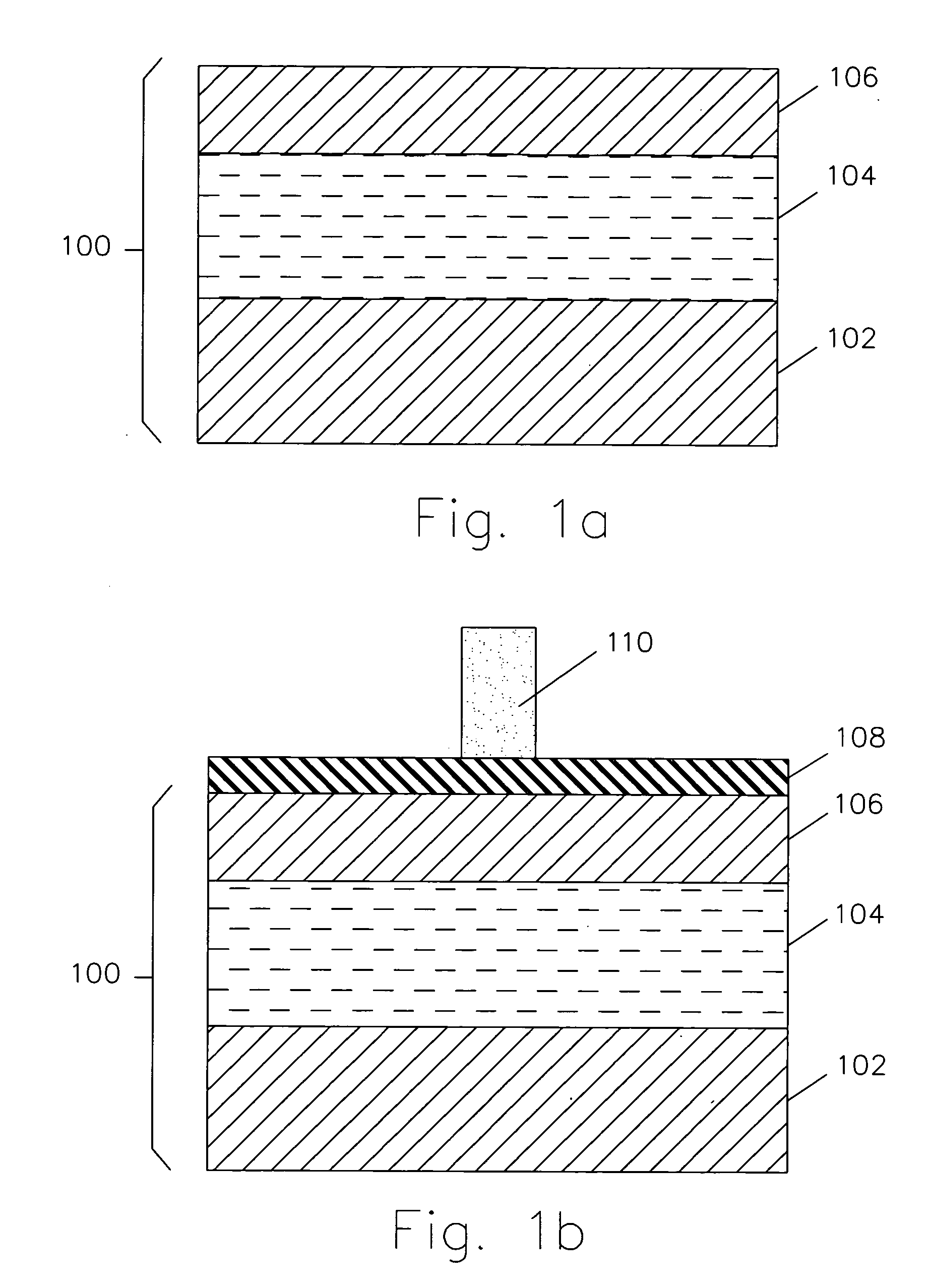
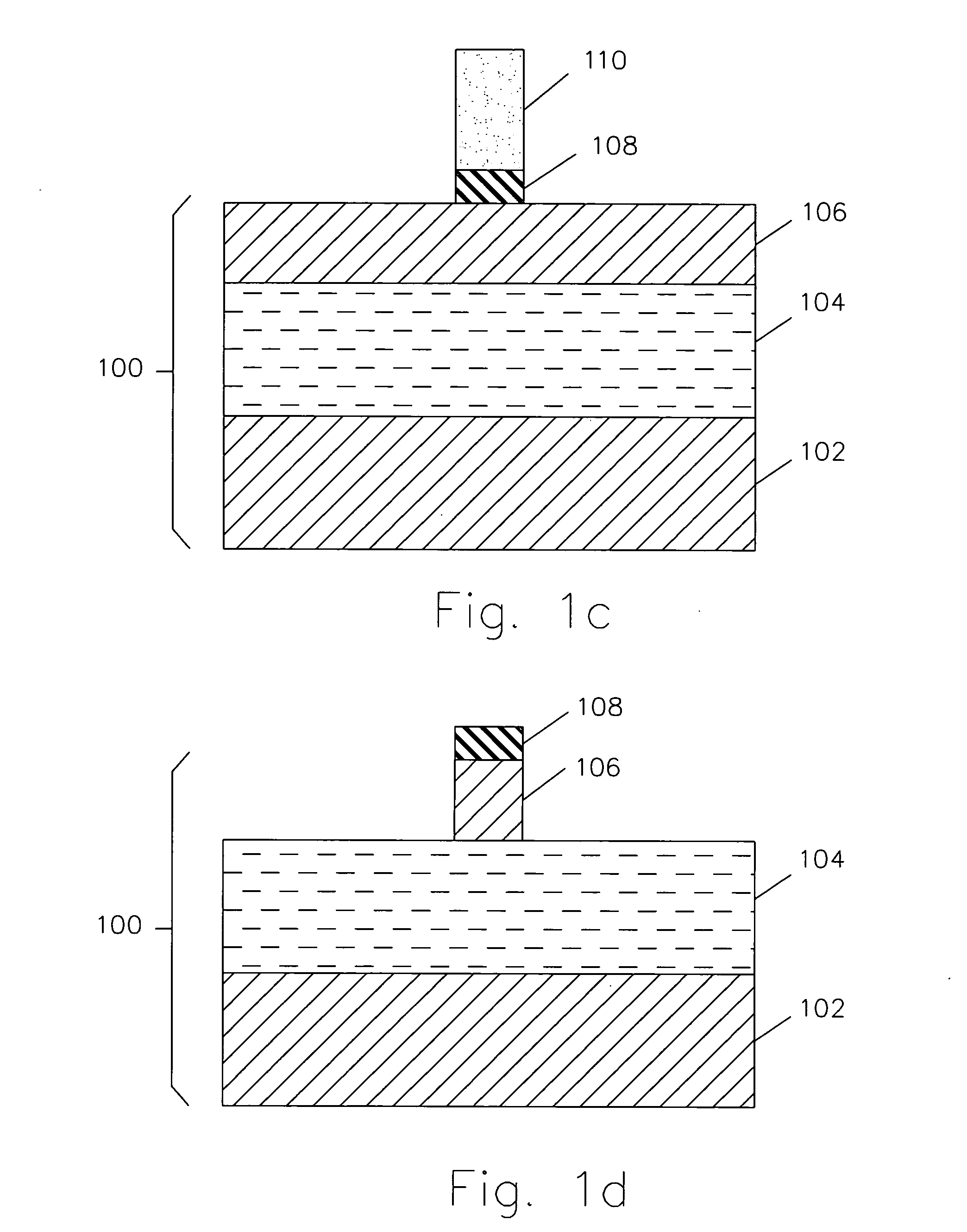
[0020] The present invention may be readily configured to any of a variety of device designs and / or methods for forming the same. Further, it will be understood by one of ordinary skill in the art that the present invention is not limited to the specific structures shown in the drawings, as the shown structures are for purposes of illustration only. It will also be understood by one of ordinary skill in the art that the present invention is not limited to the specific fabrication steps detailed herein. For example, it is not necessary to use a hard mask to define the fin.

[0021] Referring now to the drawings and, in particular, to FIG. 2, a method for forming a FinFET in accordance with an illustrative embodiment of the present invention is shown and generally represented by reference numeral 200. Method 200 may form a FinFET with any number and / or combination of other structures by: providing an appropriate substrate, such as, for example, an SOI substrate; forming one or more vert...


PUM


Abstract

There is provided a method for fabricating a FinFET in which a self-limiting reaction is employed to produce a unique and useful structure that may be detectable with simple failure analysis techniques. The structure is an improved vertical fin with a gently sloping base portion that is sufficient to reduce or prevent the formation of an undercut area in the base of the vertical fin. The structure is formed via the self-limiting properties of the reaction so that the products of the reaction form both vertically on a surface of the vertical fin and horizontally on a surface of an insulating layer (e.g., buried oxide). The products preferentially accumulate faster at the base of the vertical fin where the products from both the horizontal and vertical surfaces overlap. This accumulation or build-up results from a volume expansion stemming from the reaction. The faster accumulation in the corner areas near the base, limits the reaction first in the base region, thereby etching less material and forming the remaining, un-etched material into the sloping dielectric base.

Description

BACKGROUND OF THE INVENTION [0001] 1. Field of the Invention [0002] The present invention relates to semiconductor manufacturing. More particularly, the present invention relates to the manufacture of field effect transistors (FETs) having vertical fins (FinFETs). [0003] 2. Description of the Prior Art [0004] A FinFET is known in the art to be the simplest double gate structure to manufacture. Hence, the FinFET is a promising candidate to achieve ultimate device scaling. [0005] In a FinFET, a vertical fin is defined to form the body of a transistor. Gates can be formed on one or both sides of the vertical fin. When both sides of the vertical fin have a gate formed thereon, the transistor is generally referred to as a double-gate FinFET. A double-gate FinFET helps suppress short channel effects (SCE), reduce leakage, and enhance switching behavior. Also, a double-gate FinFET can increase gate area, which can in turn improve current control, without increasing gate length. [0006] Curr...

Claims


Application Information

Patent Timeline
IPC IPC(8): H01L21/336H01L21/84H01L29/786H01L31/0392
CPCH01L29/785H01L29/66795
Inventor NATZLE, WESLEYDORIS, BRUCE B.
Owner GLOBALFOUNDRIES INC
Why Eureka
Try Eureka