

Ultra-thin wafer handling system
- Summary
- Abstract
- Description
- Claims
- Application Information
AI Technical Summary
Benefits of technology
Problems solved by technology
Method used
Image

Examples
Embodiment Construction
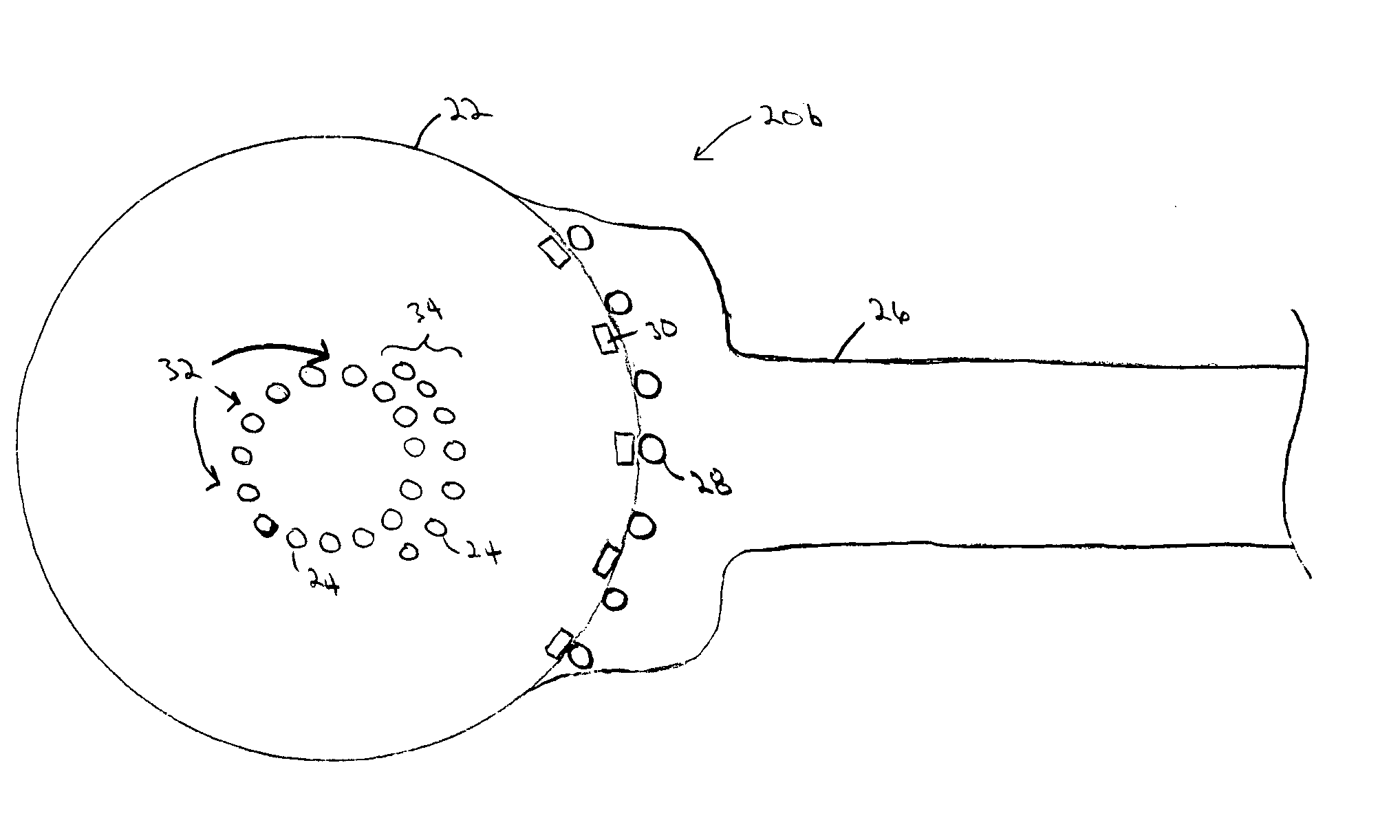
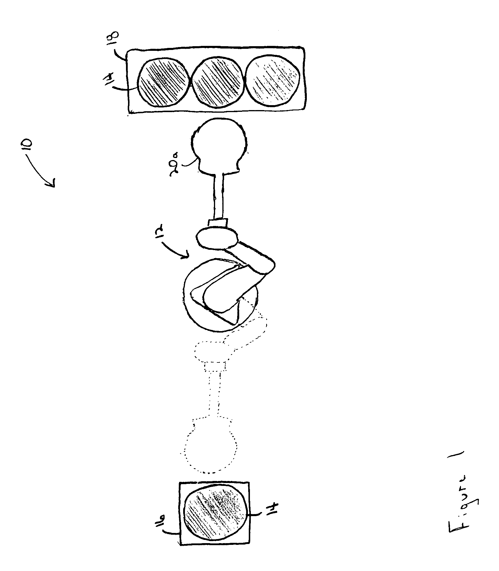
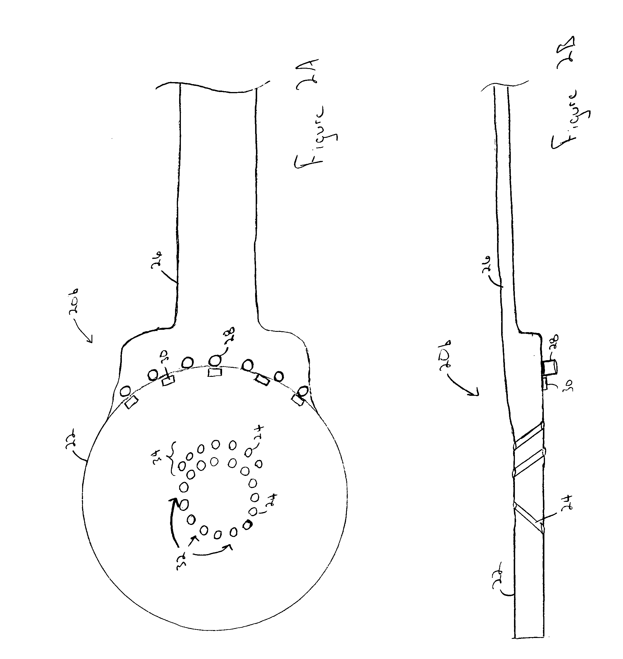
[0028]FIG. 1 is a top view of an embodiment of a substrate handling system 10 that may benefit from features of the invention. Such a system 10 may be a component piece or tool of an in-line processing apparatus, e.g., described in U.S. Pat. No. 6,217,272 to Felsenthal et al. and U.S. Pat. No. 6,530,733 to Klein et al., the entire disclosures of which are hereby incorporated by reference. The system10 includes a robot arm 12 that transports a substrate 14 or a batch of substrates 14 from a substrate carrier 16 and places them on a substrate handling structure 18 (e.g., a wafer tray or any type of substrate carrier known in the art). The substrates 14 may be, e.g., semiconductor wafers or glass substrates. The diameter of the substrates 14 may be, e.g., about 125 mm, about 150 mm, about 200 mm, about 250 mm, or about 300 mm. The thickness of the substrates 14 may be between about 10 μm and about 750 μm. Typical dimensions of an ultra-thin wafer are a diameter of about 150 mm and a th...
PUM
 Abstract
Description
Claims
Application Information