Integrated circuit with controllable test access to internal analog signal pads of an area array

a controllable, integrated circuit technology, applied in the direction of solid-state device testing/measurement, semiconductor/solid-state device testing/measurement, instruments, etc., can solve the problems of affecting the performance of analog signals, the probe card of the wire-type wafer cannot contact the peripheral bonding pads, and the inability to reach the bonding pads, etc., to achieve efficient test access, avoid excessive cost and other difficulties, and improve the effect of analog signal performan

Inactive Publication Date: 2005-05-26
AVAGO TECH INT SALES PTE LTD
View PDF20 Cites 10 Cited by
  • Summary
  • Abstract
  • Description
  • Claims
  • Application Information

AI Technical Summary

Benefits of technology

[0015] Advantageously, the invention in an illustrative embodiment allows efficient test access to internal analog signal pads of an integrated circuit die, without the excessive cost and

Problems solved by technology

A problem associated with use of area array buffers such as those shown in FIG. 2 is that it is difficult to gain access to internal analog signal pads during testing that occurs before the integrated circuit die is packaged.
Unfortunately, a standard wire-type wafer probe card can only contact the peripheral bonding pads, and cannot reach the bonding pads which are inside the area array.
Although there is another type of wafer probe card, known as a membrane probe ca

Method used


Image

  • Integrated circuit with controllable test access to internal analog signal pads of an area array
  • Integrated circuit with controllable test access to internal analog signal pads of an area array
  • Integrated circuit with controllable test access to internal analog signal pads of an area array

Examples


Embodiment Construction

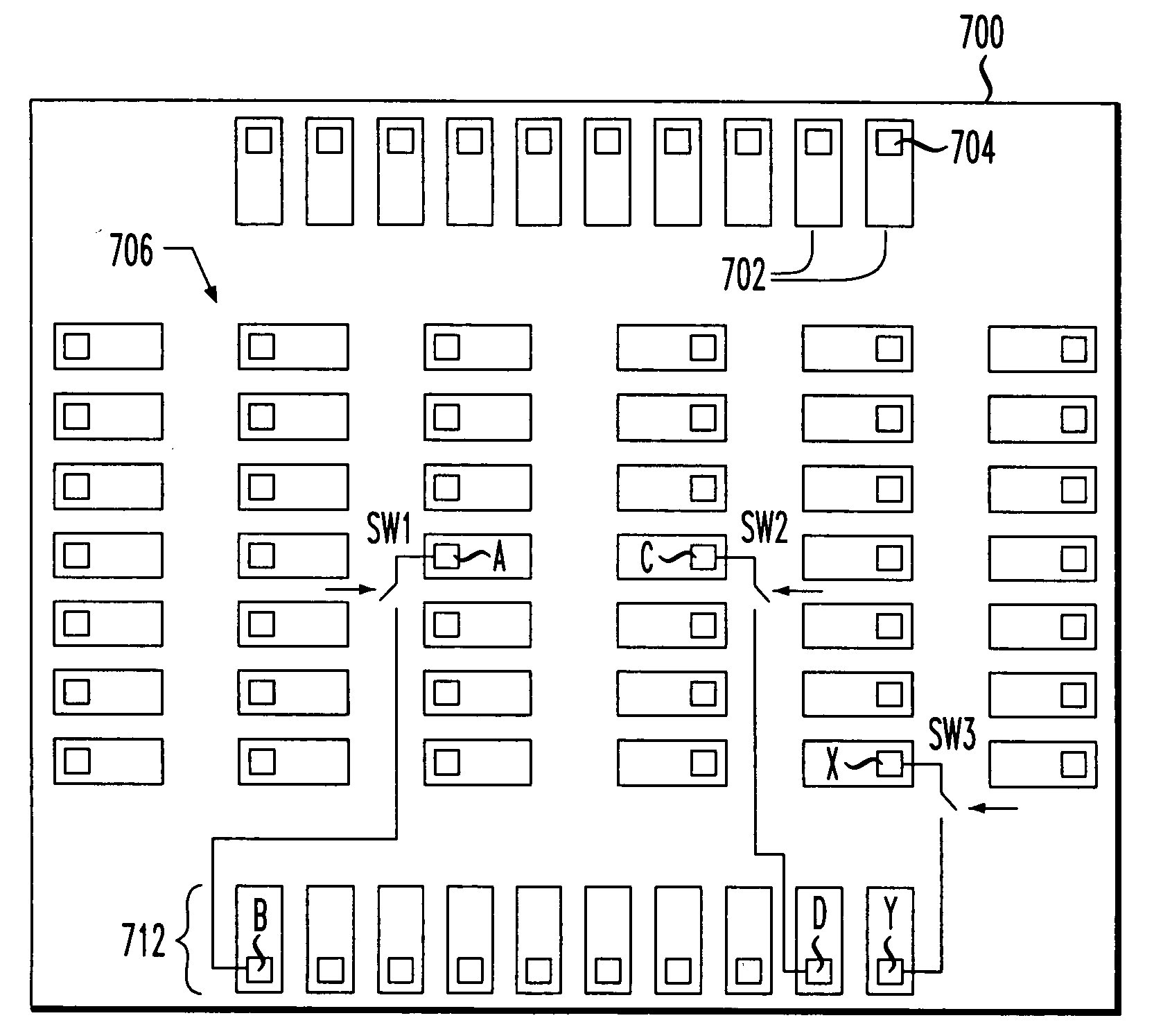
[0023] The present invention will be illustrated herein in the context of a number of exemplary integrated circuit dies, and test applications involving wafer-level testing of such dies using a wire-type wafer probe card. It should be understood, however, that the particular arrangements shown are provided by way of illustrative example only, and not intended to limit the scope of the invention in any way. As will become apparent, the techniques of the invention are utilizable in a wide variety of other integrated circuit test applications in which it is desirable to obtain access to internal analog signal pads of an integrated circuit area array, or other types of internal signal pads of an integrated circuit.

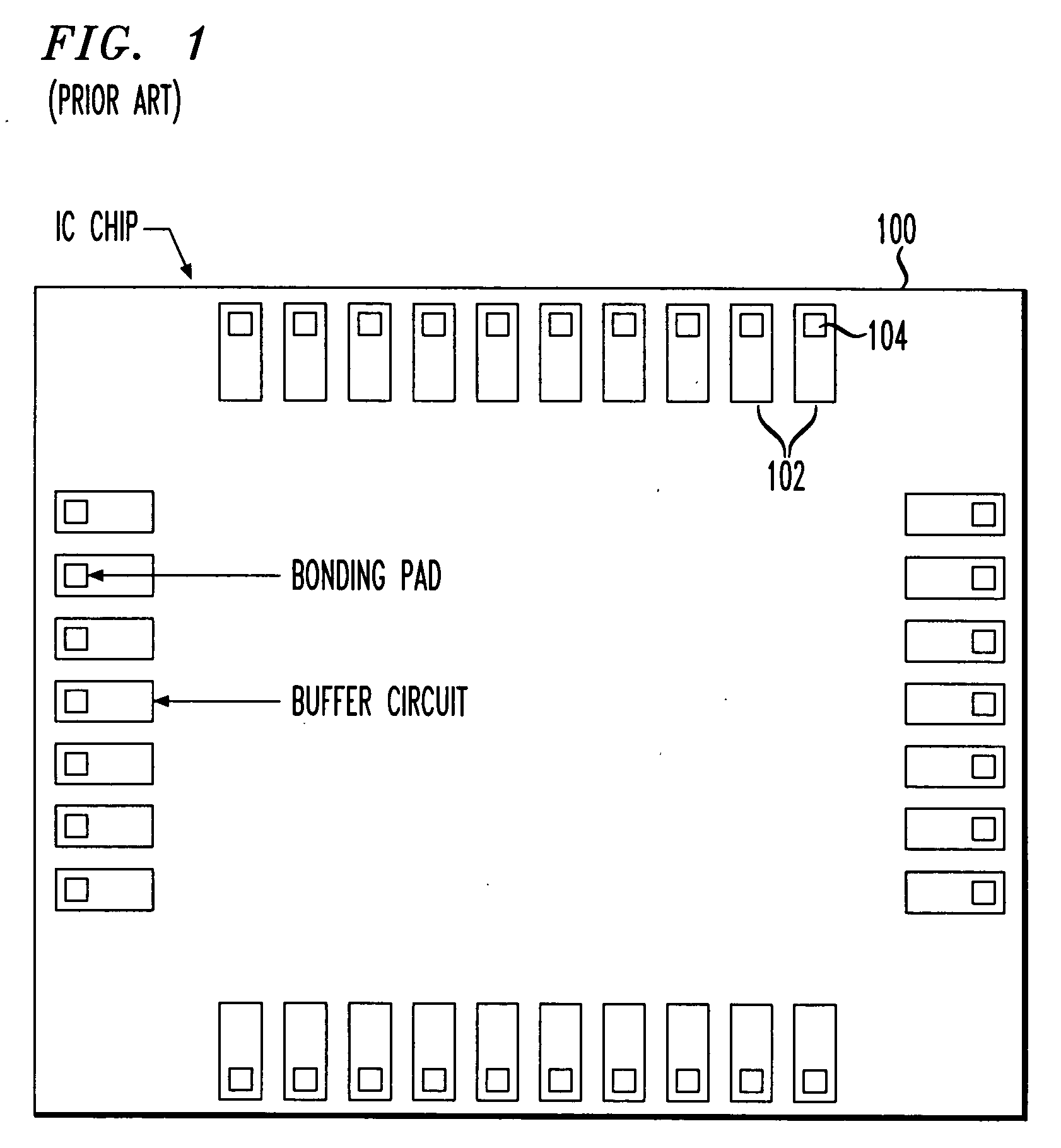
[0024] The term “internal signal pad” as used herein is intended to include a bonding pad or other type of signal pad that is arranged at a location away from a periphery of an integrated circuit die. For example, such a signal pad may be associated with a non-peripheral buff...


PUM


Abstract

An integrated circuit die comprises an internal signal pad arranged at a location away from a periphery of the die, a peripheral signal pad arranged proximate the periphery of the die, and a switch coupled between the internal signal pad and the peripheral signal pad. The switch is configurable in at least a first state in which the internal signal pad is not operatively connected to the peripheral signal pad, and a second state in which the internal signal pad is operatively connected to the peripheral signal pad, responsive to a control signal having one of respective first and second signal characteristics. The switch is configured in the first state during normal operation of the integrated circuit die, and is configured in the second state to permit test access to the internal signal pad via the peripheral signal pad.

Description

FIELD OF THE INVENTION [0001] The present invention relates generally to integrated circuits, and more particularly to techniques for providing test access to internal signal pads of an area array or other internal portions of an integrated circuit die. BACKGROUND OF THE INVENTION [0002] Integrated circuits have to be able to send and to receive electrical signals to and from external or “off-chip” elements. This communication with off-chip elements is typically achieved through the use of buffer circuits, also commonly referred to simply as “buffers.”FIGS. 1 and 2 show the layouts of conventional integrated circuits, illustrating the placement of buffer circuits therein. [0003] With reference initially to FIG. 1, an integrated circuit die 100 includes a plurality of buffer circuits 102 arranged adjacent to its periphery as shown. Associated with each of the buffer circuits 102 is a corresponding bonding pad 104, which may be viewed as an example of what is more generally referred t...

Claims


Application Information

Patent Timeline
IPC IPC(8): H01L27/00G01R31/28H01L21/66H01L21/822H01L27/04
CPCG01R31/2884H01L27/00
Inventor GABARA, THADDEUS JOHNHUBER, CAROL ANNMORRIS, BERNARD LEE
Owner AVAGO TECH INT SALES PTE LTD
Why Eureka
Try Eureka