

Device with switchable capacitance
- Summary
- Abstract
- Description
- Claims
- Application Information
AI Technical Summary
Benefits of technology
Problems solved by technology
Method used
Image

Examples
Embodiment Construction
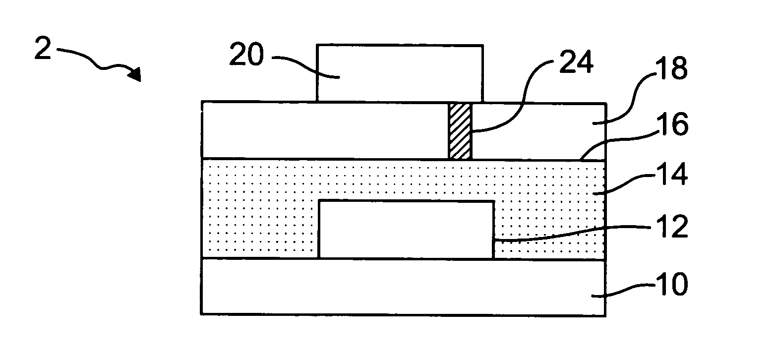
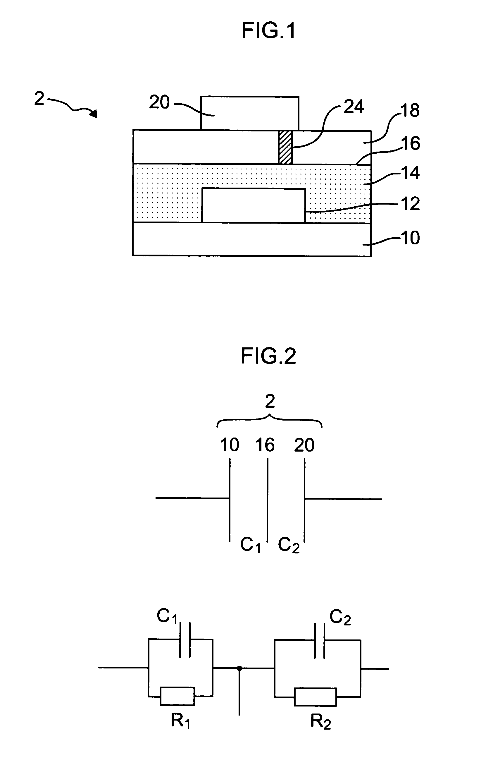
[0028]FIG. 1 is a schematic sectional view of a capacitor 2 according to a first preferred embodiment of the present invention. On a substrate 10, a stack-like arrangement of a first capacitor electrode 12, a dielectric layer 14, an intermediate layer 16, a switching member 18 and a second capacitor electrode 20 is formed. The first capacitor electrode 12 and the second capacitor electrode 20 are herein also referred to as first electrode 12 and second electrode 20, respectively. The first capacitor electrode 12 and the second capacitor electrode 20 and the intermediate electrode 16 between the capacitor electrodes 12, 20 are essentially in parallel to each other and separated from each other by the dielectric layer 14 and the switching member 18, respectively. The first capacitor electrode 12, the intermediate electrode 16 and the second capacitor electrode 20 at least partially overlap, and preferentially at least the capacitor electrode 12, 20 essentially completely overlap. This...
PUM
 Abstract
Description
Claims
Application Information