

Hybrid latch flip-flop
- Summary
- Abstract
- Description
- Claims
- Application Information
AI Technical Summary
Benefits of technology
Problems solved by technology
Method used
Image

Examples
first embodiment
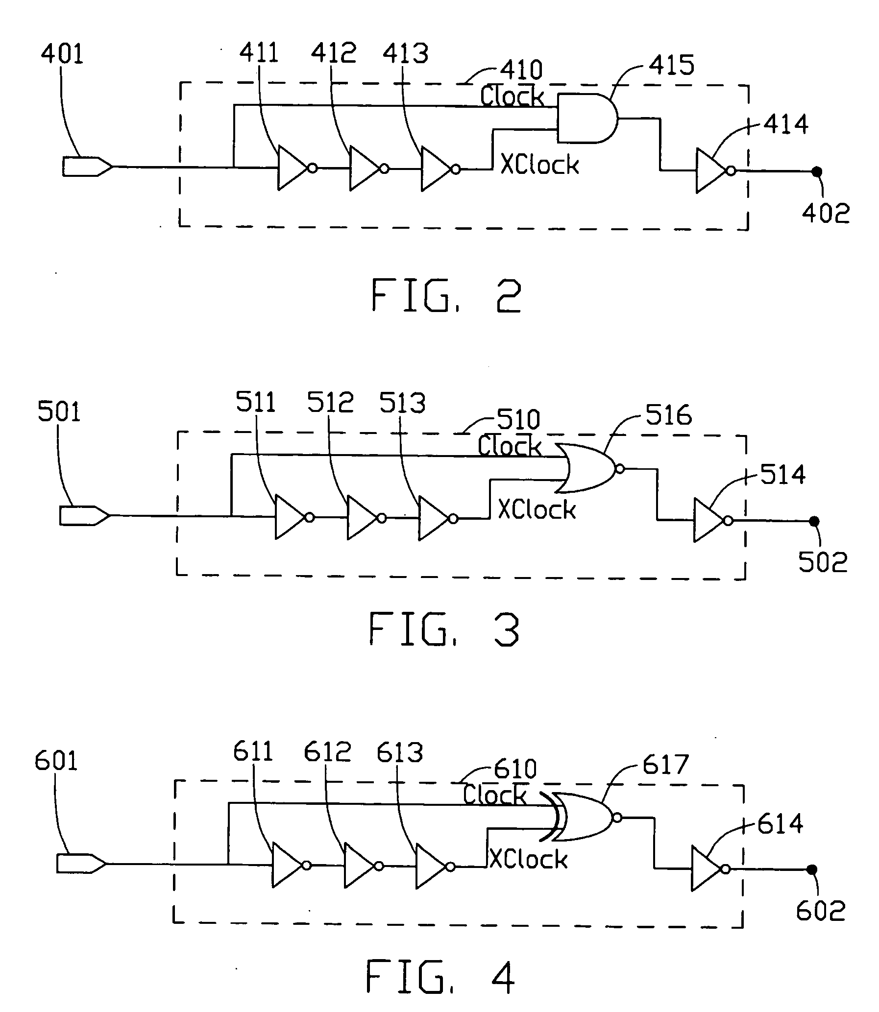
[0038] Referring to FIG. 2, this is a circuit diagram of the negative pulse generating unit of FIG. 1. The negative pulse generating unit 410 includes a first inverter 411, a second inverter 412, a third inverter 413, a fourth inverter 414, and an AND gate 415. The input of the first inverter 411 is connected to the clock input 401. The output of the first inverter 411 is connected to the input of the second inverter 412. The output of the second inverter 412 is connected to the input of the third inverter 413. The output of the third inverter 413 is connected to one input of the AND gate 415. The other input of the AND gate 415 is connected to the clock input 401. The output of the AND gate 415 is connected to the input of the fourth inverter 414. The output of the fourth inverter 414 is connected to the node 402. The first inverter 411 and the second inverter 412 are used for delaying the clock signal, and the third inverter 413 is used for delaying and inverting the clock signal ...
second embodiment
[0039] Referring to FIG. 3, this is a circuit diagram of the negative pulse generating unit of FIG. 1. The negative pulse generating unit 510 includes a first inverter 511, a second inverter 512, a third inverter 513, a fourth inverter 514, and a NOR gate 516. The input of the first inverter 511 is connected to the clock input 501. The output of the first inverter 511 is connected to the input of the second inverter 512. The output of the second inverter 512 is connected to the input of the third inverter 513. The output of the third inverter 513 is connected to one input of the NOR gate 516. The other input of the NOR gate 516 is connected to the clock input 501. The output of the NOR gate 516 is connected to the input of the fourth inverter 514. The output of the fourth inverter 514 is connected to the node 502. The first inverter 511 and the second inverter 512 are used for delaying the clock signal, and the third inverter 513 is used for delaying and inverting the clock signal f...
third embodiment
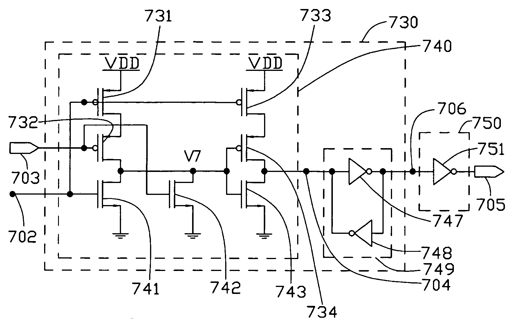
[0048] Referring to FIG. 7, this is a circuit diagram of the latch flip-flop of FIG. 1. The latch flip-flop 930 comprises a sample unit 940 and a hold unit 949. The sample unit 940 comprises: four PMOS type transistors, which are a first PMOS type transistor 931, a second PMOS type transistor 932, a third PMOS type transistor 933, and a fourth PMOS type transistor 934; and two NMOS type transistors, which are a first NMOS type transistor 941 and a second NMOS type transistor 942. The hold unit 949 includes a fifth inverter 947 and a sixth inverter 948.
[0049] The source of first PMOS type transistor 931 and the source of the third PMOS type transistor 933 are connected to a power source VDD. The gate of the first PMOS type transistor 931, the gate of the first NMOS type transistor 941, and the gate of the third PMOS type transistor 933 are connected to the node 902. The gate of the second PMOS type transistor 932 is connected to the data input 903. The drain of the first PMOS type tr...
PUM
 Abstract
Description
Claims
Application Information