CMOS pixel with dual gate PMOS

Inactive Publication Date: 2005-03-22
UNITED MICROELECTRONICS CORP
View PDF6 Cites 6 Cited by
  • Summary
  • Abstract
  • Description
  • Claims
  • Application Information

AI Technical Summary

Benefits of technology

Active pixel sensors, APS, are of particular value in digital imaging systems because they can be fabricated using standard CMOS, complimentary metal oxide semiconductor, processing and because they have lower power consumption than CCD, charge coupled device, imagers. As CMOS process parameters shrink, the analog performance of minimum size transistors deterior

Problems solved by technology

As CMOS process parameters shrink, the analog performance of minimum size transistors deter

Method used


Image

  • CMOS pixel with dual gate PMOS
  • CMOS pixel with dual gate PMOS
  • CMOS pixel with dual gate PMOS

Examples


Example

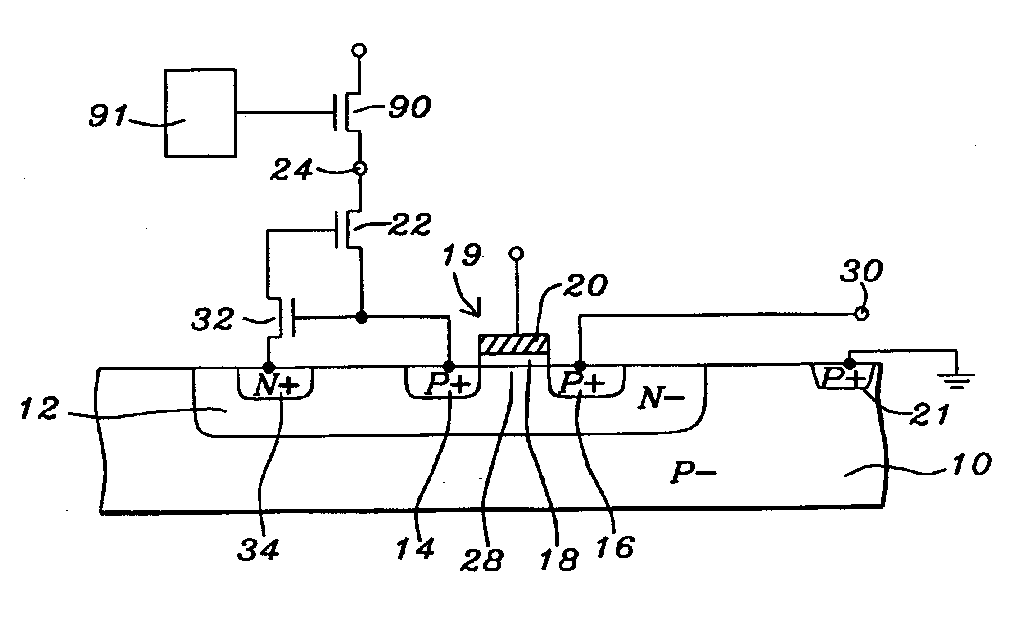
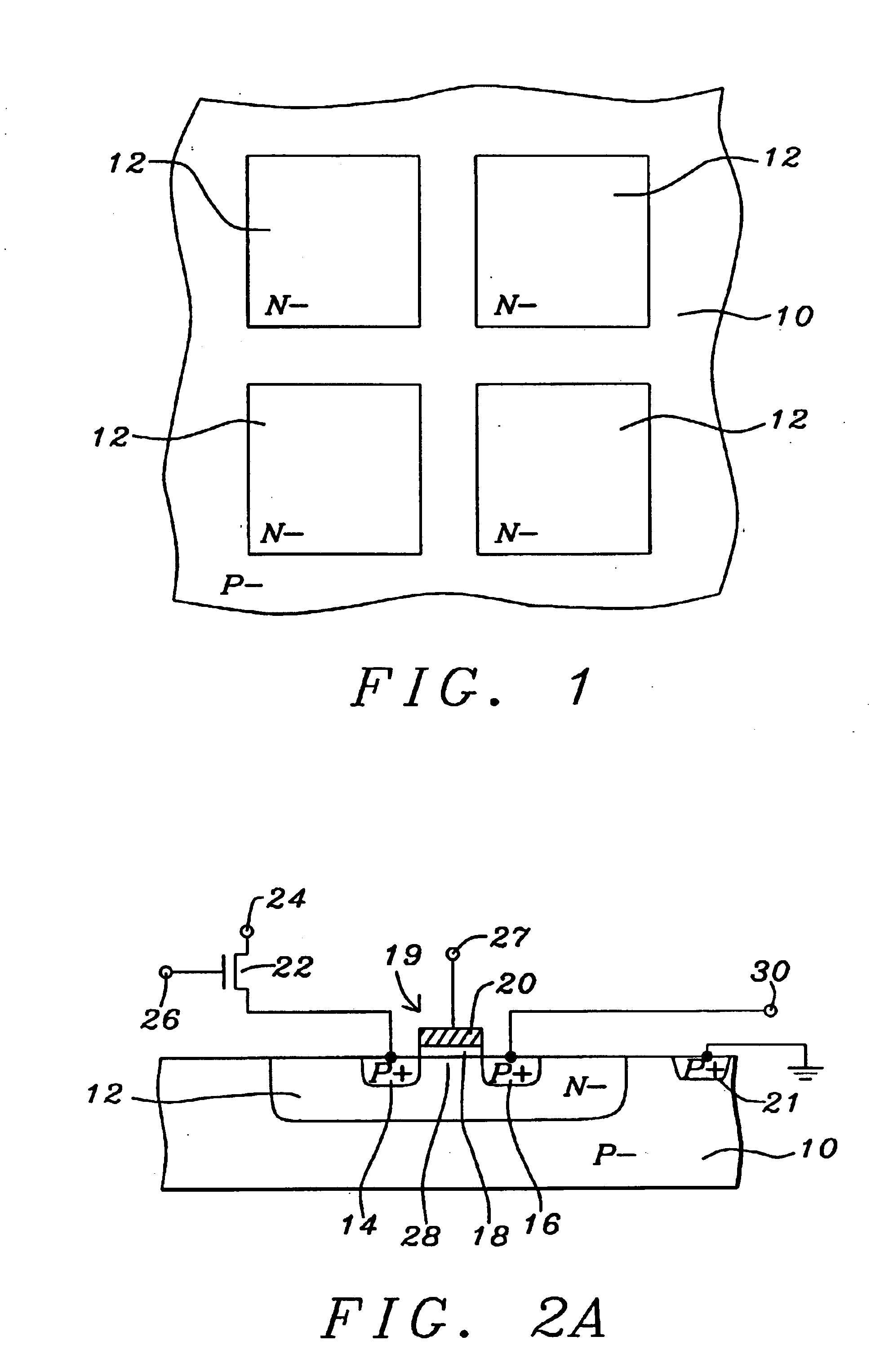
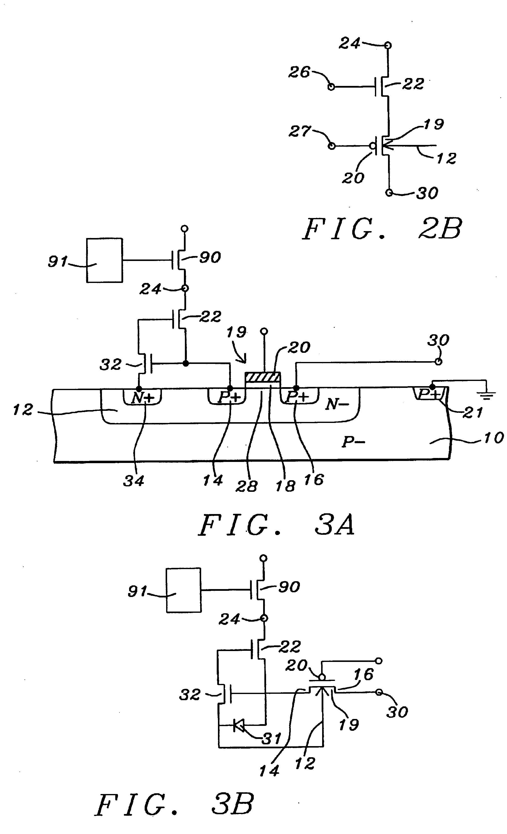
Refer now to FIGS. 1-4B of the drawings for a description of the preferred embodiments of this invention. FIG. 1 shows a top view of a number of N− wells 12 formed of N− type silicon in a P− type silicon substrate 10. Typically, but not necessarily, the P− type silicon substrate 10 is a P− type epitaxial silicon layer. FIG. 1 shows four N− wells 12 as an example however the actual number will be larger or smaller, typically smaller, arranged in an array. Each N− well 12 forms a PN junction diode with the surrounding P− silicon material. The N− wells 12 are biased such that the potential of the N− wells 12 are higher than the P− silicon material 10 and the PN junction is back biased. This back biased PN junction forms a pixel which can accumulate carriers generated by an external signal to be read during a readout period. Typically, but not necessarily, the external signal is optical radiation and the carriers are photo-generated carriers.

FIG. 2A shows a cross section view of one of ...


PUM


Abstract

A pixel circuit with a dual gate PMOS is formed by forming two P+ regions in an N well. The N well is in a P type substrate. The two P+ regions form the source and drain of a PMOS transistor. The PMOS transistors formed within the N well will not affect the collection of the photo-generated charge as long as the source and drain potentials of the PMOS transistors are set at a lower potential than the N well potential so that they remain reverse biased with respect to the N well. One of the P+ regions used to form the source and drain regions can be used to reset the pixel after it has been read in preparation for the next cycle of accumulating photo-generated charge. The N well forms a second gate for the dual gate PMOS transistor since the potential of the N well 12 affects the conductivity of the channel of the PMOS transistor. The addition of two NMOS transistors enables the readout signal to be stored at the gate of one of the NMOS transistors thereby making a snapshot imager possible. The circuit can be expanded to form two PMOS transistors sharing a common drain in the N well.

Description

BACKGROUND OF THE INVENTION(1) Field of the InventionThis invention relates to a CMOS pixel comprising an N− well formed in a P− epitaxial silicon layer with a dual gate PMOS transistors formed in the N− well.(2) Description of the Related ArtU.S. Pat. No. 6,147,362 to Keyser describes a high performance pixel for active matrix electronic displays. The pixel combines a compact mesa-isolated PMOS access transistor with a novel, area efficient high voltage device.U.S. Pat. No. 6,127,697 to Guidash describes an active pixel sensor comprising a substrate of a first conductivity type having a surface containing PMOS and NMOS implants that are indicative of a sub-micron CMOS process, a photodetector formed at a first depth from an implant of a second conductivity type that is opposite the first conductivity type on the surface, and a gate on the surface adjacent to the photodetector. The photodetector is formed by an implant of the second conductivity type that is deeper and more lightly ...

Claims


Application Information

Patent Timeline
IPC IPC(8): H01L29/76H01L21/70H01L27/146H01L29/02H01L29/10H01L29/66H01L21/8238H01L27/085H01L31/036H01L31/101H01L27/092H01L31/113H01L31/10H01L31/112
CPCH01L27/14609H01L31/112H01L27/14643H01L27/14632E02F5/305
Inventor DOSLUOGLU, TANERMCCAFFREY, NATHANIEL JOSEPH
Owner UNITED MICROELECTRONICS CORP
Why Eureka
Try Eureka