
Display device, driving method thereof and electronic appliance

Inactive Publication Date: 2006-08-03
SEMICON ENERGY LAB CO LTD
View PDF3 Cites 5 Cited by
  • Summary
  • Abstract
  • Description
  • Claims
  • Application Information

AI Technical Summary

Benefits of technology

[0011] The invention is made to solve the abovementioned problems and to increase a yield by not generating a luminescent spot but generating a dark spot even if a short circuit is caused between the source and the drain of the TFT connected to the EL element in series.
[0041] Further, in the case where a transistor operates with a source potential being close to a low potential side power source, the transistor is desirably an n-channel transistor. Conversely, in the case where a transistor operates with a source potential being close to a high potential side power source, the transistor is desirably a p-channel transistor. By employing such a structure, an absolute value of a voltage between a gate and source of a transistor can be made larger. Therefore, the transistor can easily be used as a switch. Note that a CMOS switching element may be constructed by using both an n-channel transistor and a p-channel transistor.
[0045] Further, in the invention, a voltage signal is used as a video signal so that a structure of a driver circuit for inputting a video signal to a pixel can be simplified.
[0046] Further, in the fifth to eighth structures of the invention, a transistor arranged in each pixel functions as a mere switching element, therefore, power consumption of a display device can be lowered.

Problems solved by technology

Since the luminance of an EL element is proportional to a current value of the EL element, an EL display device using an EL element as a display element has a problem of off current of a switching element in the case where a power source line is connected to the EL element through the switching element.
If a certain pixel of a display device continuously emits light regardless of a video signal, that is, even if one luminescent spot is generated, the display device is often determined to be defective.
On the other hand, if a certain pixel always emits no light regardless of a video signal, that is, if a few dark spots are generated, a display device is not determined to be defective.

Method used


Image

  • Display device, driving method thereof and electronic appliance
  • Display device, driving method thereof and electronic appliance
  • Display device, driving method thereof and electronic appliance

Examples


embodiment mode 1

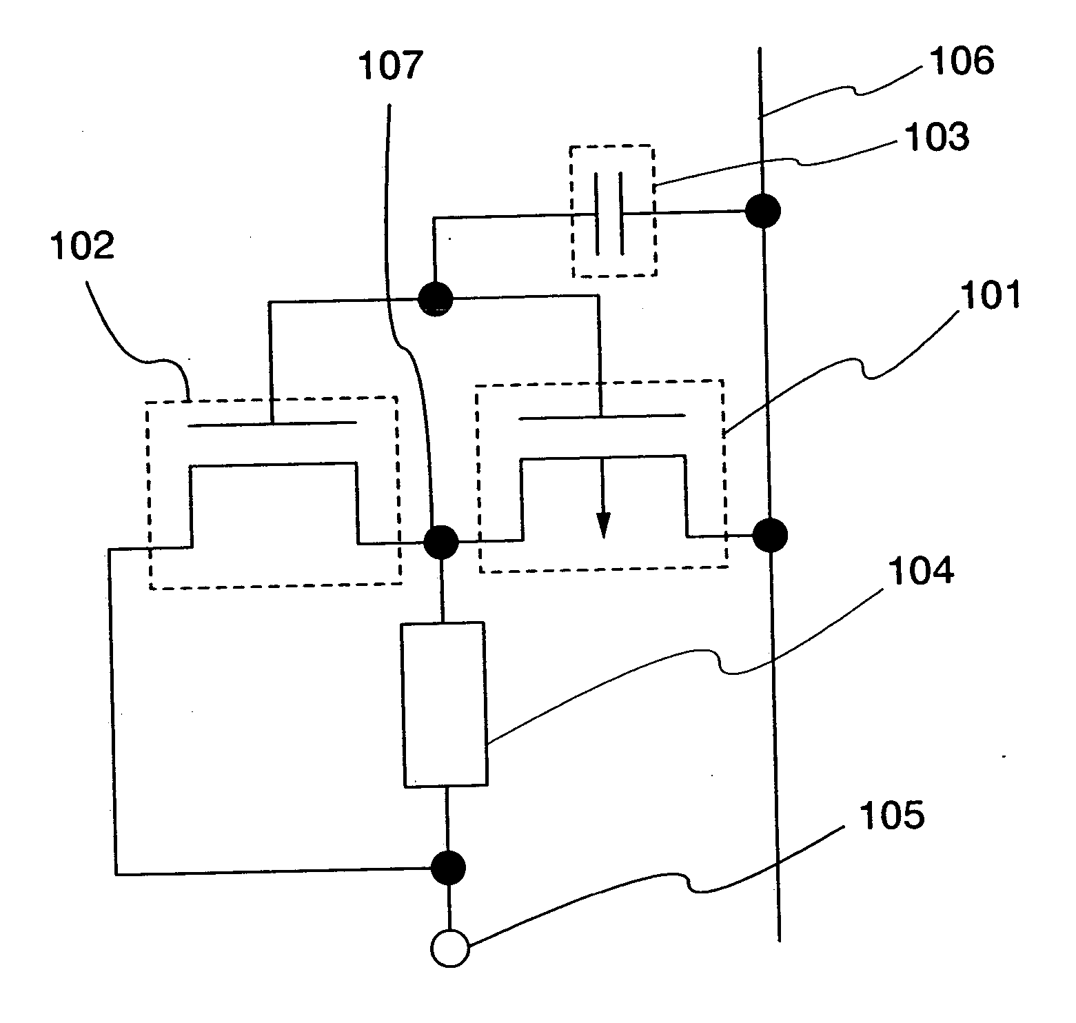
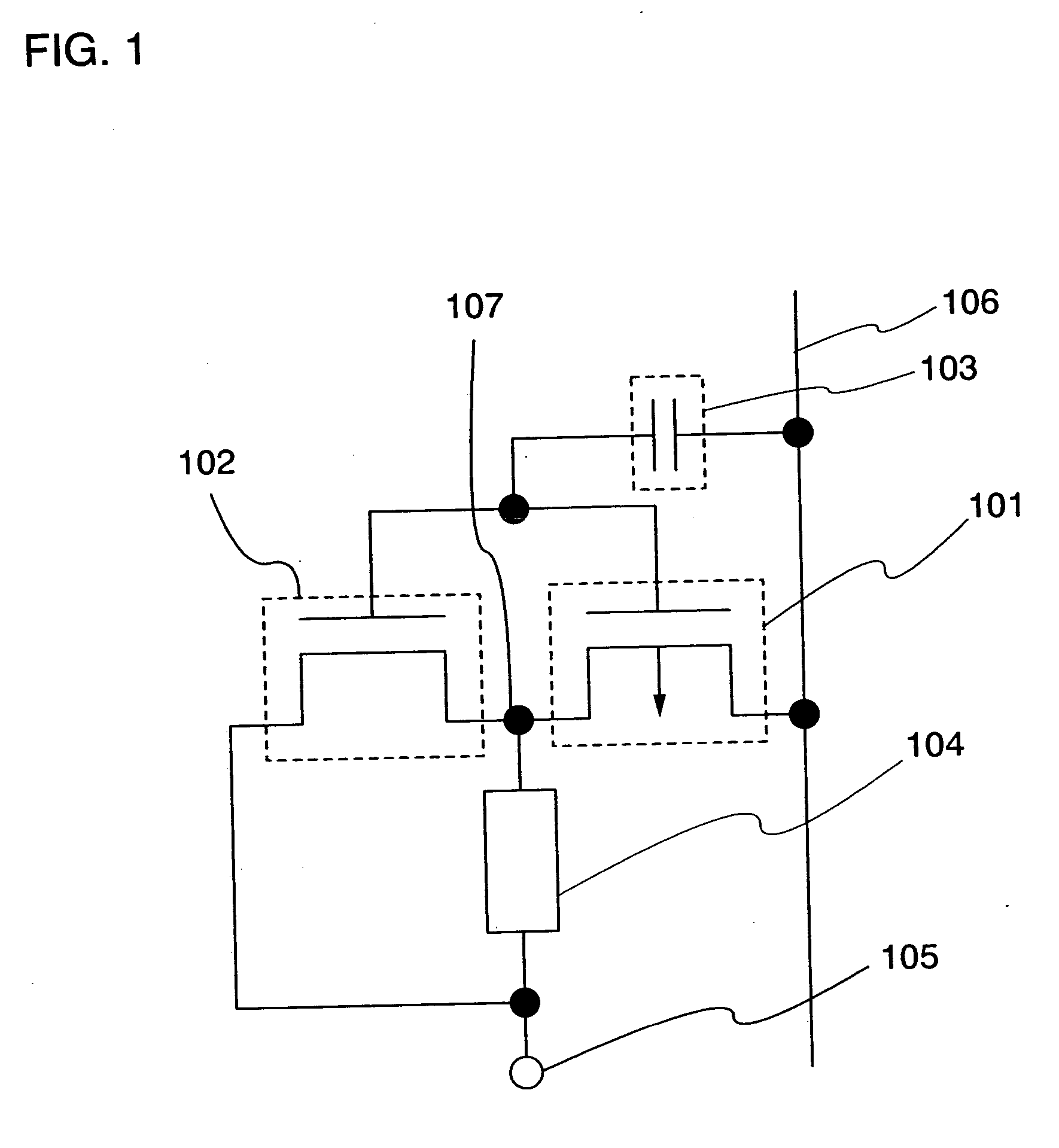
[0061] Description is made on a pixel structure of the display device of the fifth structure with reference to FIG. 1.

[0062] In FIG. 1, reference numerals 101 and 102 are TFTs, 103 is a capacitor, 104 is a light-emitting element, 105 is a counter electrode, that is the other electrode of a pair of electrodes of the light-emitting element 104, and 106 is a power source line.

[0063] Each pixel includes the capacitor 103, the light-emitting element 104, and the TFTs 101 and 102.

[0064] The power source line 106 is connected to one of a source electrode and a drain electrode of the TFT 101, the other of the source electrode and the drain electrode of the TFT 101 is connected to one electrode of the light-emitting element 104 and one of a source electrode and a drain electrode of the TFT 102, the other of the source electrode and the drain electrode of the TFT 102 is connected to the other electrode of the light-emitting element 104, gate electrodes of the TFTs 101 and 102 are connected...

embodiment mode 2

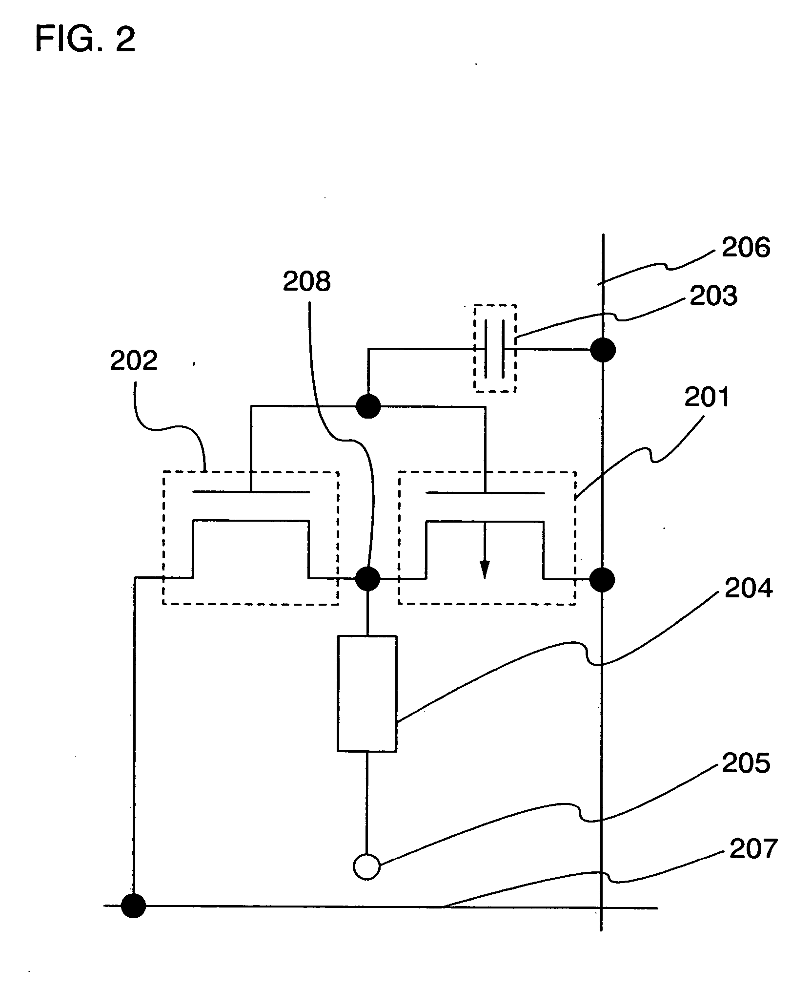
[0078] Description is made on a pixel structure of the display device of the sixth structure with reference to FIG. 2.

[0079] In FIG. 2, reference numerals 201 and 202 are TFTs, 203 is a capacitor, 204 is a light-emitting element, 205 is a counter electrode, that is the other electrode of a pair of electrodes of the light-emitting element 204, and 206 and 207 are power source lines.

[0080] Each pixel includes the capacitor 203, the light-emitting element 204, and the TFTs 201 and 202.

[0081] The power source line 206 is connected to one of a source electrode and a drain electrode of the TFT 201, the other of the source electrode and the drain electrode of the TFT 201 is connected to one electrode of the light-emitting element 204 and one of a source electrode and a drain electrode of the TFT 202, the other of the source electrode and the drain electrode of the TFT 202 is connected to the power source line 207, gate electrodes of the TFTs 201 and 202 are connected to one electrode of...

embodiment mode 3

[0093] Description is made on a pixel structure of the display device of the seventh structure with reference to FIG. 3.

[0094] In FIG. 3, reference numerals 301, 302, and 303 are TFTs, 304 is a capacitor, 305 is a light-emitting element, 306 is a counter electrode, that is the other electrode of a pair of electrodes of the light-emitting element 305, 307 is a power source line, 308 is a source signal line, and 309 is a gate select line.

[0095] Each pixel includes the capacitor 304, the light-emitting element 305, and the TFTs 301, 302, and 303.

[0096] The power source line 307 is connected to one of a source electrode and a drain electrode of the TFT 301, the other of the source electrode and the drain electrode of the TFT 301 is connected to one electrode of the light-emitting element 305 and one of a source electrode and a drain electrode of the TFT 302, the other of the source electrode and the drain electrode of the TFT 302 is connected to the other electrode of the light-emitt...


PUM


Abstract

A display device with high productivity and high display quality and a driving method thereof are provided by suppressing generation of a luminescent spot. A first switching element and a second switching element each of which has a different polarity are disposed in series between a power source line for supplying power to a light-emitting element and a power source line having a potential which is equal to or lower than a threshold voltage of the light-emitting element; one electrode of the light-emitting element is connected to a connecting node of the two switching elements; and in the case where a potential which is equal to or higher than the threshold voltage of the light-emitting element is applied to the light-emitting element regardless of an on / off state of the first switching element, a potential applied to the light-emitting element is set to be lower than the threshold voltage by turning the second switching element on. Thus, generation of a luminescent spot is prevented.

Description

BACKGROUND OF THE INVENTION [0001] 1. Field of the Invention [0002] The present invention relates to an active matrix display device and a driving method thereof. In particular, the invention relates to a display device having a switching element such as a thin film transistor (hereinafter referred to as TFT) and a light-emitting element in each pixel and the driving method thereof Further, the invention relates to an electronic appliance using the display device and the driving method thereof. [0003] 2. Description of the Related Art [0004] In recent years, the technique for forming TFTs has largely progressed, and is applied and developed to active matrix display devices. Particularly, since the field effect mobility (also referred to as mobility) of a TFT using a polysilicon film as an active layer is higher than that of a conventional TFT using an amorphous silicon film, high-speed operations are enabled. Therefore, a pixel can be controlled by a driver circuit which is formed u...

Claims


Application Information

Patent Timeline
IPC IPC(8): G09G3/36
CPCG09G3/3233G09G3/3258G09G2300/0842G09G2320/0238G09G2330/02G09G2330/10H01L27/3244H10K59/12
Inventor UMEZAKI, ATSUSHI
Owner SEMICON ENERGY LAB CO LTD
Learn More