Mammography apparatus and detecting unit

Inactive Publication Date: 2005-05-26
FUJIFILM HLDG CORP +1
8 Cites 24 Cited by

AI-Extracted Technical Summary

Problems solved by technology

However, no mammography apparatus has been disclosed to date that enables solid state detectors of various sizes to be utilized interchangeably.
Consequently, a problem arises in that it becomes difficult for the X-ra...

Method used

[0045] The aforementioned X-ray dosage detector 10 is stacked on top of the solid state detector 20, and configured to be positioned between the X-ray source 2 and the solid state detector 20 when the film cassette 8 is held on the imaging table 4. For this reason, the X-ray dosage detector 10 is capable of directly detecting the X-rays emitted from the X-ray source, without the solid state detector 20 acting as an intermediary. Therefore, the X-ray dosage can be accurately measured, without being influenced by the solid state detector 20. In addition, because the X-ray dosage detector 10 is formed on a resin substrate 15, which has a lower X-ray absorption rate than glass substrates, adver...

Benefits of technology

[0011] The present invention has been developed in view of the above circumstances. It is an object of the present invention to provide a mammography apparatus that employs solid state detectors as X-ray image detecting means, in which solid state det...

Abstract

Detection accuracy of X-ray dosages, to be applied to control the amount of irradiated X-rays, is improved in a mammography apparatus that employs solid state detectors as X-ray image detecting means, and that is capable of interchangeably utilizing solid state detectors of various sizes, without adversely influencing detection of images by the solid state detector. A solid state detector, for recording image information by receiving irradiation of X-rays that bear the image information, and for outputting image signals that represent the recorded image information, an X-ray dosage detector, for detecting the amount of irradiated X-rays, and a moving grid, for removing scattered radiation, are housed within a detecting unit, stacked in this order. The detecting unit is configured to be removably attachable to an imaging table of a mammography apparatus. Thereby, interchangeable use of detecting units having solid state detectors of various sizes housed therein is enabled.

Application Domain

DosimetersPhotometry +4

Technology Topic

Solid state detectorX ray image +9

Image

  • Mammography apparatus and detecting unit
  • Mammography apparatus and detecting unit
  • Mammography apparatus and detecting unit

Examples

  • Experimental program(1)

Example

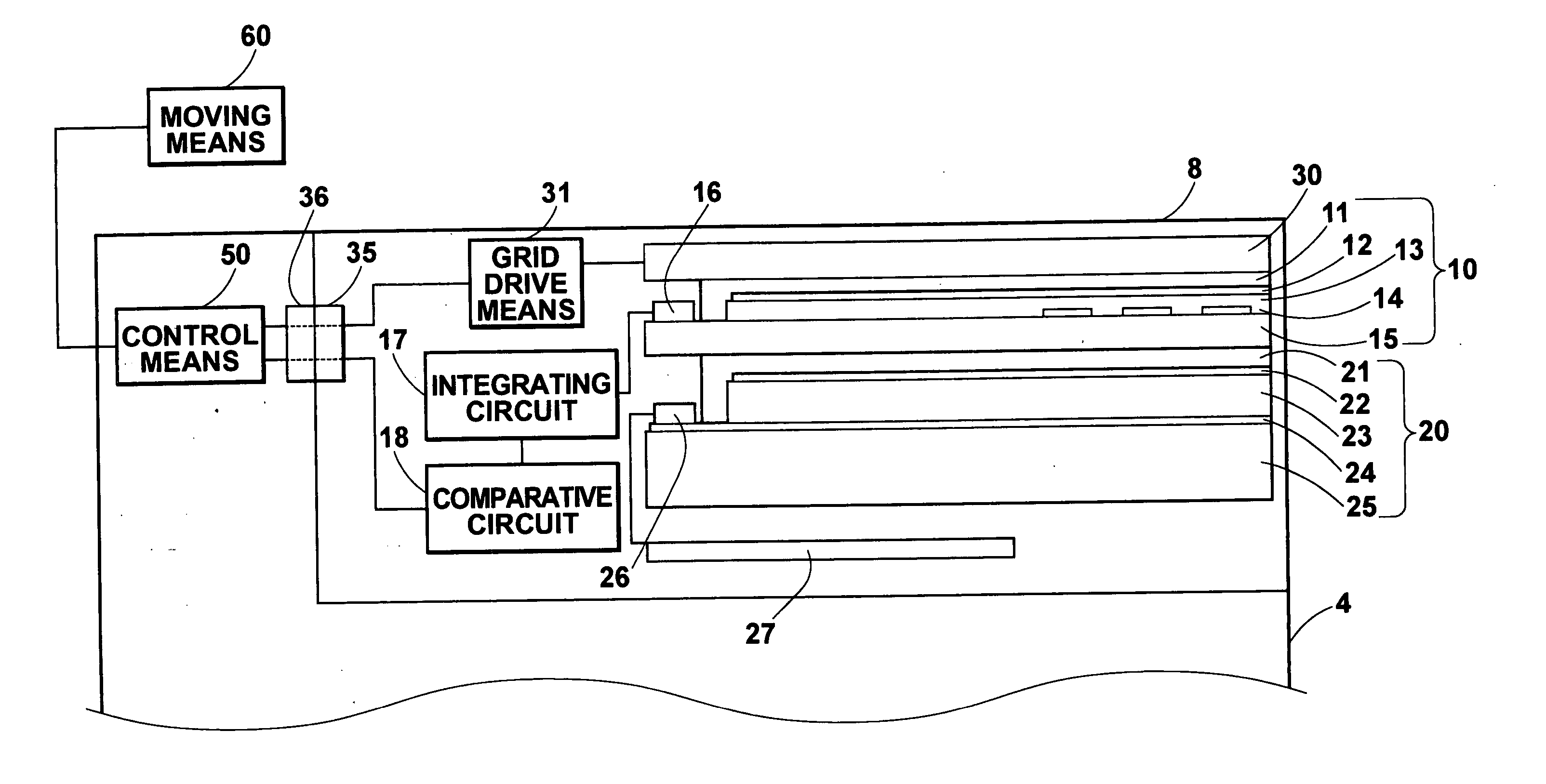
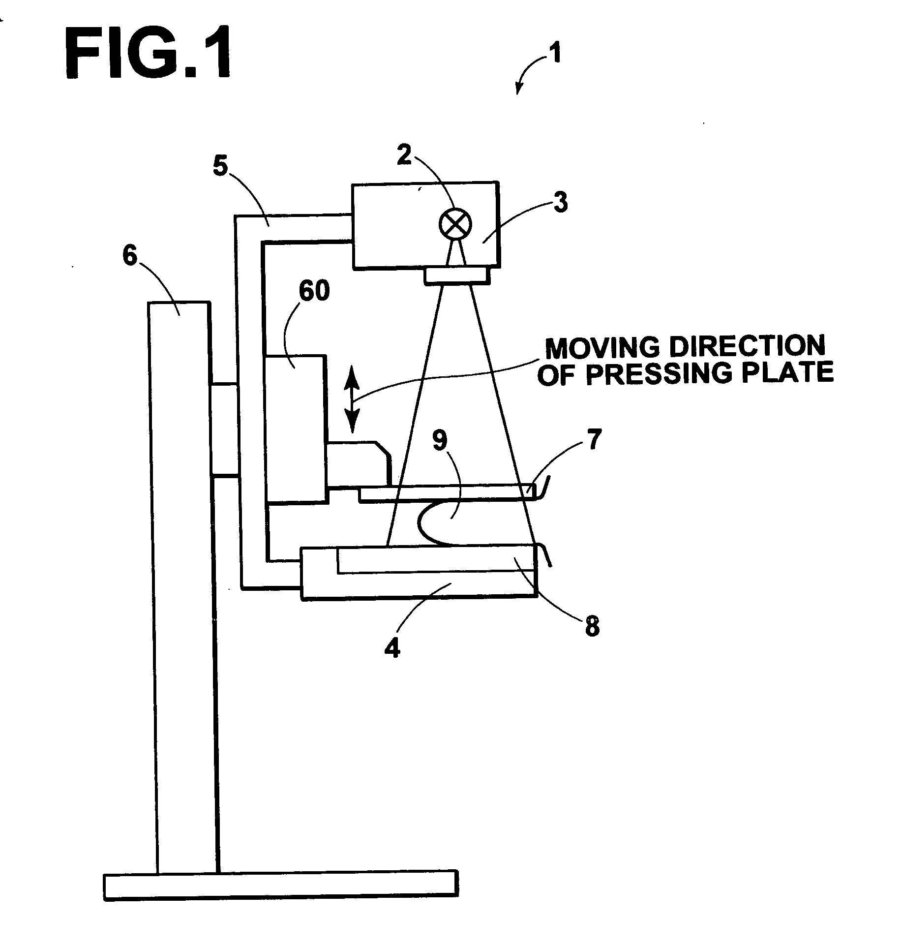
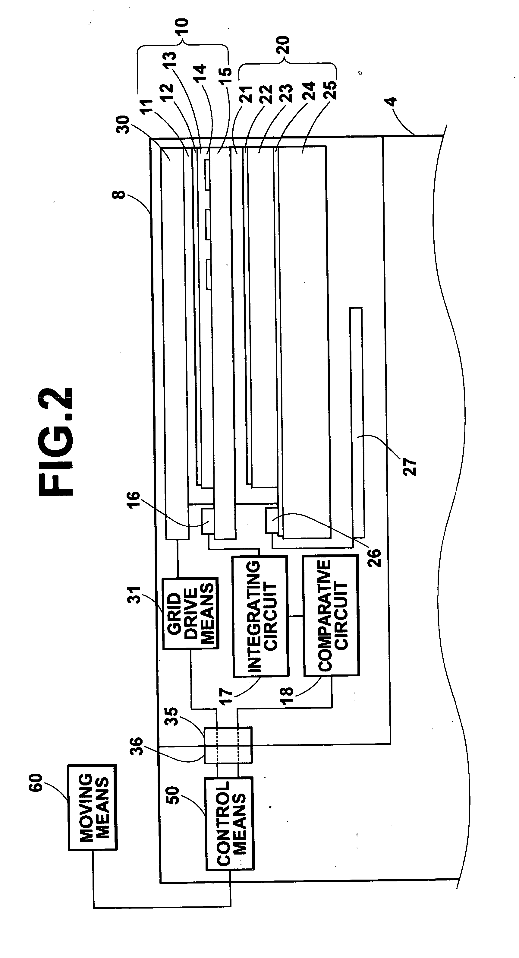
[0033] Hereinafter, an embodiment of the present invention will be described in detail with reference to the attached drawings. FIG. 1 is a schematic diagram that illustrates an example of a mammography apparatus according to the present invention. FIG. 2 is a schematic diagram that illustrates the interior of a detecting unit of the mammography apparatus. FIG. 3 is a schematic diagram illustrating a conductive layer portion of an X-ray dosage detector of the mammography apparatus. FIG. 4 is a circuit diagram illustrating an integrating circuit and a comparative circuit of the mammography apparatus.
[0034] A mammography apparatus 1 comprises: an X-ray source housing portion 3 that houses an X-ray source 2 within its interior; an imaging table 4 for holding a detecting unit 8; arms 5; and a base 6. The X-ray source housing portion 3 and the imaging table 4 are linked by the arms 5 so that they face each other. The arms are mounted on the base 6.
[0035] Further, a pressing plate 7, for pressing and holding a subject's breast 9 from above, and a pressing plate moving means 60, for moving the pressing plate 7 automatically in response to commands from a control means 50, are mounted on the arms 5. The pressing plate moving means 60 is constituted by a linear motor (not shown). The pressing plate moving means 60 moves the pressing plate 7 reciprocally between a first position, at which the breast 9 is pressed against the detecting unit 8 held on the imaging table 4, and a second position, at which the pressure is released.
[0036] An X-ray dosage detector 10, for detecting the dosage of X-rays irradiated on the detecting unit 8; a solid state detector 20, which is an imaging device; a moving grid 30, for removing scattered radiation; a grid drive means 31, for driving the moving grid 30; and a power source (not shown), for supplying electricity to the above components, are provided within the detecting unit 8.
[0037] The X-ray dosage detector comprises: a first conductive layer 14; a photoconductive layer 13 that generates electrical charges and exhibits conductivity when irradiated with X-rays; a second conductive layer 12; and an insulative layer 11, stacked in this order on a resin substrate 15.
[0038] The first conductive layer 14 comprises a plurality of conductive layer portions 14a, which are formed separated from each other, as illustrated in FIG. 3. Each of the conductive layer portions 14a is connected to an IC chip 16. Further, the IC chip 16 is connected to an integrating circuit 17, and the integrating circuit 17 is connected to a comparative circuit 18.
[0039] The X-ray dosage detector 10 operates in the following manner. Electric fields are formed between each of the conductive layer portions 14a of the first conductive layer 14 and the second conductive layer 12. If X-rays are irradiated onto the photoconductive layer 13 at this time, charge pairs are generated within the photoconductive layer 13. Current corresponding to the amount of charge pairs flows between each conductive layer portion 14a and the second conductive layer 12, and the current is converted to voltage by the IC chip 16.
[0040] The integrating circuit 17 converts the current that flows between each conductive layer portion 14a and the second conductive layer 12 into voltages, and integrates the converted voltages. In the case that the voltages integrated by the integrating circuit 17 exceed a predetermined value, the comparative circuit 18 outputs data indicating this fact. Thereby, judgment can be made regarding whether the X-ray dosage irradiated on the film cassette 8 has exceeded a predetermined value.
[0041] Note that the judgment regarding whether the X-ray dosage irradiated on the film cassette 8 has exceeded the predetermined value may be made based on the current that flows between any one of the plurality of conductive layer portions 14a and the second conductive layer 12, or based on the total current that flows between each of the plurality of conductive layer portions 14a and the second conductive layer 12.
[0042] The solid state detector 20 comprises: a first conductive layer 24 formed of a—Si TFT's; a photoconductive layer 23 that exhibits conductivity by generating charges when irradiated with X-rays; a second conductive layer 22; and an insulative layer 21, which are stacked in this order on a glass substrate 25.
[0043] A TFT is formed corresponding to each pixel in the first conductive layer 24. Output from each TFT is connected to an IC chip 26, and the IC chip 26 is connected to a printed circuit board 27, which is equipped with an A/D converting portion, a memory, and the like (not shown).
[0044] The solid state detector 20 operates in the following manner. An electric field is formed between the first conductive layer 24 and the second conductive layer 22. If X-rays are irradiated onto the photoconductive layer 23 at this time, charge pairs are generated within the photoconductive layer 23. Latent image charges corresponding to the amount of charge pairs are accumulated within the first conductive layer 24. When reading out the accumulated latent image charges, the TFT's of the first conductive layer 24 are sequentially driven to read out the latent image charges corresponding to each pixel. Thereby, an electrostatic latent image borne by the latent image charges are read out.
[0045] The aforementioned X-ray dosage detector 10 is stacked on top of the solid state detector 20, and configured to be positioned between the X-ray source 2 and the solid state detector 20 when the film cassette 8 is held on the imaging table 4. For this reason, the X-ray dosage detector 10 is capable of directly detecting the X-rays emitted from the X-ray source, without the solid state detector 20 acting as an intermediary. Therefore, the X-ray dosage can be accurately measured, without being influenced by the solid state detector 20. In addition, because the X-ray dosage detector 10 is formed on a resin substrate 15, which has a lower X-ray absorption rate than glass substrates, adverse influences on detection of X-ray images by the solid state detector 20 are reduced. Accordingly, the image quality of images detected by the solid state detector 20 is improved. Note that a carbon plate or aluminum oxides may be employed as the material of the substrate, as alternatives to resin.
[0046] Here, a description will be given of the photoconductive layer 13 and the photoconductive layer 23, which are employed in the X-ray dosage detector 10 and the solid state detector 20, respectively.
[0047] The X-ray spectra commonly emitted from X-ray sources is not uniform at all X-ray energies. The X-ray absorption coefficient differs for X-ray energies, depending on the material that constitutes a photoconductive layer. For these reasons, in the case that the photoconductive layer 13 of the X-ray dosage detector 10 and the photoconductive layer 23 of the solid state detector 20 are formed by different materials, there is a possibility that the spectrum of the X-rays, which pass through the X-ray dosage detector 10 and which are detected by the solid state detector 20, will change drastically within the X-ray dosage detector 10. If such a change in the X-ray spectrum occurs, there is a possibility that adverse influences will be imparted on the detection of X-ray images by the solid state detector 20.
[0048] Therefore, in the present embodiment, both the photoconductive layer 13 of the X-ray dosage detector 10 and the photoconductive layer 23 of the solid state detector 20 are constituted by a—Se. Thereby, adverse influences imparted on the detection of X-ray images by the solid state detector 20 are reduced, and the image quality of images detected by the solid state detector 20 is improved.
[0049] The mammography apparatus 1 comprises the control means 50, for controlling the X-ray source 2, the pressing plate moving means 60, the grid drive means 31 and the like. The detecting unit 8 is equipped with a connector 35, for engaging a connector 36, which is provided on the imaging table 4. The grid drive means 31 and the comparative circuit 18 are connected to the control means 50 via the connectors 35 and 36, while the detecting unit 8 is held on the imaging table 4.
[0050] By adopting the construction described above, it becomes possible to removably attach the detecting unit 8 to the imaging table 4. Therefore, detecting units 8 that house solid state detectors 20 of various sizes, corresponding to the size of a subject's breast, can be interchangeably used.
[0051] Next, the operation of the mammography apparatus 1, which is constructed as described above, will be described. FIG. 5 is a timing chart of each operation of the mammography apparatus, from imaging to readout.
[0052] During imaging, the control means drives the pressing plate moving means 60 to move the pressing plate 7 to the first position at which a breast 9 is pressed, based on commands which are manually input by an operator. Thereby, the breast 9 is fixed on the film cassette 8.
[0053] Next, the operator presses a first step of a two step irradiation switch (not shown), and the control means 50 causes the grid drive means 31 to drive the moving grid 30 and cancels resetting of the integrating circuit 17.
[0054] Thereafter, the operator presses the second step of the irradiation switch, and the control means 50 causes the X-ray source 2 to emit X-rays onto the breast 9. The X-rays, which have passed through the breast 9, that is, the X-rays that bear X-ray image information of the breast 9, are irradiated on the detecting unit 8. These X-rays are detected by each of the conductive layer portions 14a of the X-ray dosage detector, and voltages corresponding to the X-ray dosage are integrated by the integrating circuit 17. Latent image charges that bear the X-ray image information are accumulated within the solid state detector 20. The amount of accumulated latent image charges is substantially proportional to the X-ray dosage which has passed through a subject. Therefore, the latent image charges bear the electrostatic latent image.
[0055] If the output of the integrating circuit, that is, the dosage of X-rays irradiated on the detecting unit 8, exceeds a predetermined value, information indicating this fact is transmitted from the comparative circuit 18 to the control means 50, and the control means 50 stops the X-ray source when this information is received.
[0056] When the first step of the irradiation switch is released by the operator, the control means 50 causes the grid drive means 31 to stop the moving grid 30, resets the integrating circuit, and performs readout of the latent image charges from the solid state detector 20.
[0057] After readout of the latent image charges is completed, the control means drives the pressing plate moving means 60 to move the pressing plate 7 to the second position, at which the pressure on the breast .9 is released, and the process ends.
[0058] Noise becomes overlapped with the latent image charges, if vibration is imparted to the solid state detector 20 during readout of the latent image charges therefrom. However, this problem can be overcome by reading out the latent image charges from the solid state detector 20 in the manner described above.
[0059] A preferred embodiment of the present invention has been described above. However, the present invention is not limited to the above embodiment. For example, the solid state detector 20 may be that of the optical readout type. In addition, the X-ray dosage detector 10 may be formed directly on the solid state detector 20 rather than on the resin substrate 15.

PUM

no PUM

Description & Claims & Application Information

We can also present the details of the Description, Claims and Application information to help users get a comprehensive understanding of the technical details of the patent, such as background art, summary of invention, brief description of drawings, description of embodiments, and other original content. On the other hand, users can also determine the specific scope of protection of the technology through the list of claims; as well as understand the changes in the life cycle of the technology with the presentation of the patent timeline. Login to view more.
Why Eureka
Try Eureka