Self-assembled circuits and circuit patterns

a technology of circuits and patterns, applied in the field of patterns and apparatus, can solve the problems of limiting the usefulness of small patterns that might be used for the further manufacture, affecting and limiting the usefulness of small patterns that might be used for the manufacture of small patterns, etc., to achieve the effect of facilitating the attraction and binding of tiles

Inactive Publication Date: 2005-05-26
CALIFORNIA INST OF TECH
View PDF1 Cites 39 Cited by
  • Summary
  • Abstract
  • Description
  • Claims
  • Application Information

AI Technical Summary

Benefits of technology

[0009] According to one embodiment of the invention, a self-assembly method is provided for self-assembling a circuit pattern. The method includes generating a set of tiles, each of the tiles corresponding to a segment of molecules, the set of tiles comprising a set of rule tiles and a set of boundary tiles, each of the tiles having one or more binding regions; assigning a label from a set of labels to each binding region of each tile; self interacting, with attractive forces, one or more of the tiles with one or more other tiles among the set of tiles; associating using selective interaction of at least one boundary tile from the set of boundary tiles with at least one rules tile from the set of rules tiles based upon at least a first label from the one boundary tile and at least a second label from the one rules tiles; and bonding at least one binding region of the one boundary tile with at least one binding region of the one rules tile to form a first portion of a circuit pattern. According to a specific embodiment, the first label and the second label are the same. According to another specific embodiment, the method further includes associating using selective interaction the one boundary tile with at least a second boundary tile of the set of boundary tiles based upon at least a third label from the one boundary tile and a fourth label from the second boundary tile; and bonding the one boundary tile with the second boundary tile to form a second portion of the circuit structure. According to another specific embodiment, the third label and the fourth label are the same. According to another specific embodiment, the method further includes associating using selective interaction the one rules tile with at least a second rules tile of the set of rules tiles based upon at least a fifth label from the one rules tile and a sixth label from the second rules tile; and bonding the one rules tiles with the second rules tile to form a third portion of the circuit structure. According to another specific embodiment, the fifth label and the sixth label are the same. According to another specific embodiment, the set of label are a set of binding rules. According to another specific embodiment, the tiles are passive tiles. According to another specific embodiment, the circuit pattern includes at least one of a circuit pattern for a demultiplexer, a memory, a pseudowavelet matrix, a Sierpinski triangle, a binary adder, and a Hadamard matrix. According to another specific embodiment, the molecular structures include at least one of DNA (deoxyribonucleic acid) segments, proteins, porphyrins, and polydimethylsiloxane molding. According to another specific embodiment, selective interaction automatically facilitates the attraction and binding of the tiles. According to another specific embodiment, the tiles have at least one of molecular dimensions, nanometer dimensions, and micrometer dimensions.

Problems solved by technology

While AFM techniques might be of use to produce a variety of periodic and non-periodic patterns, the placement of individual atoms and / or molecules to build a small pattern tends to be relatively slow.
While chemical agents have been used to manufacture small patterns, traditional patterns formed by these techniques tend to be periodic, thus limiting their usefulness for the manufacture of small patterns that might be used for the further manufacture of devices that are non-periodic.
Creating a unique building block specifically for its position within a pattern is a tedious and time consuming process.

Method used


Image

  • Self-assembled circuits and circuit patterns
  • Self-assembled circuits and circuit patterns
  • Self-assembled circuits and circuit patterns

Examples


examples

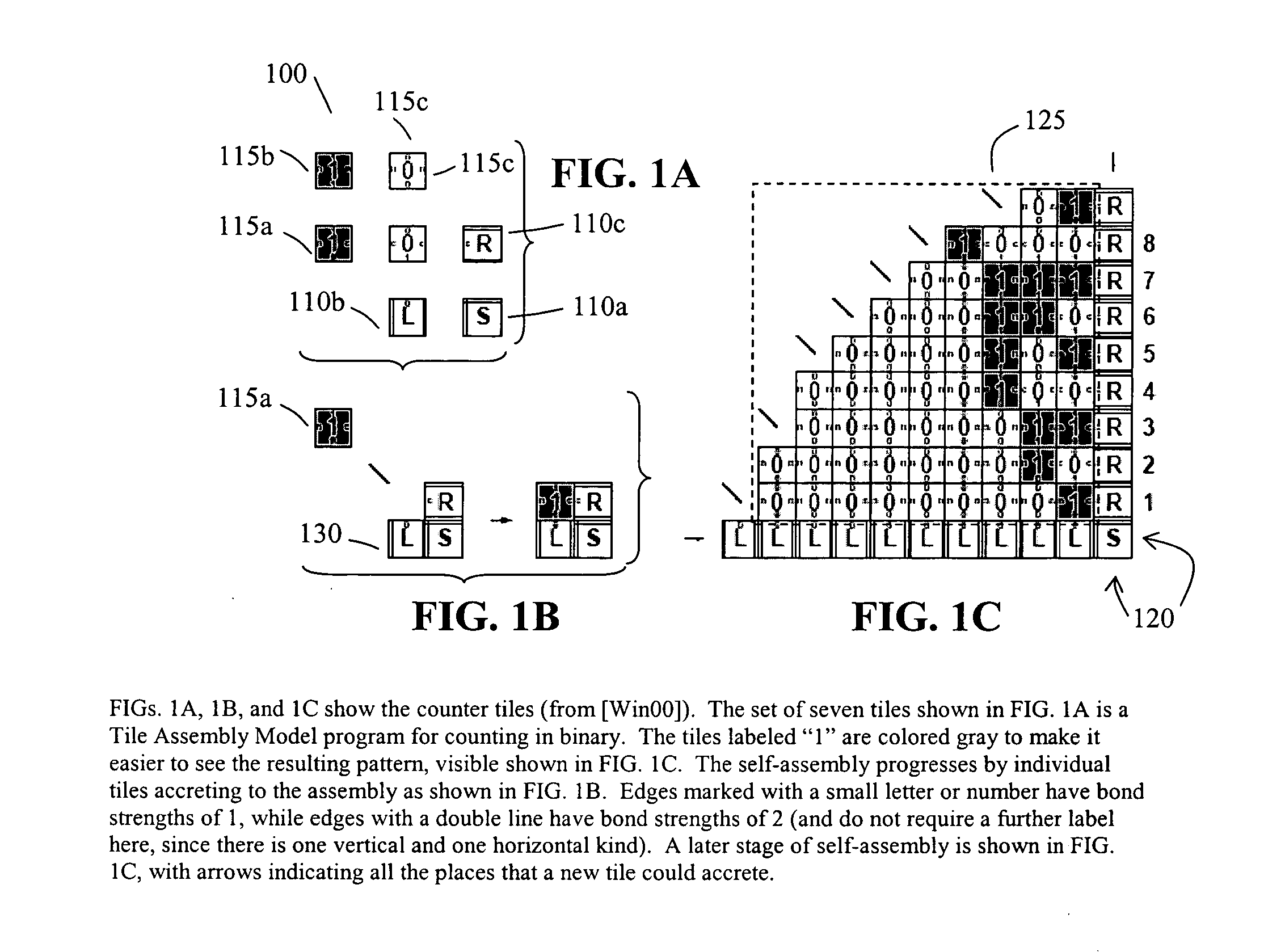
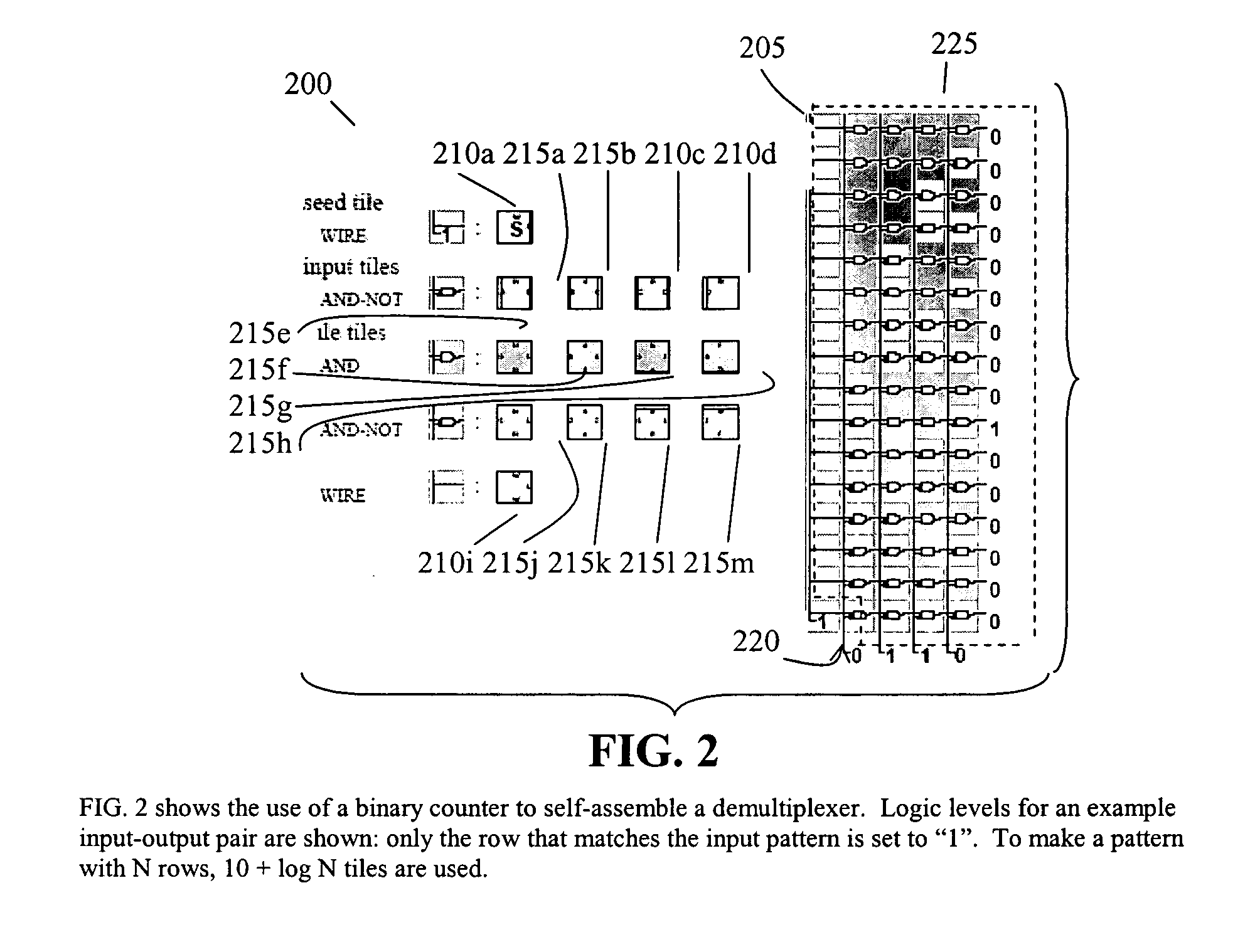
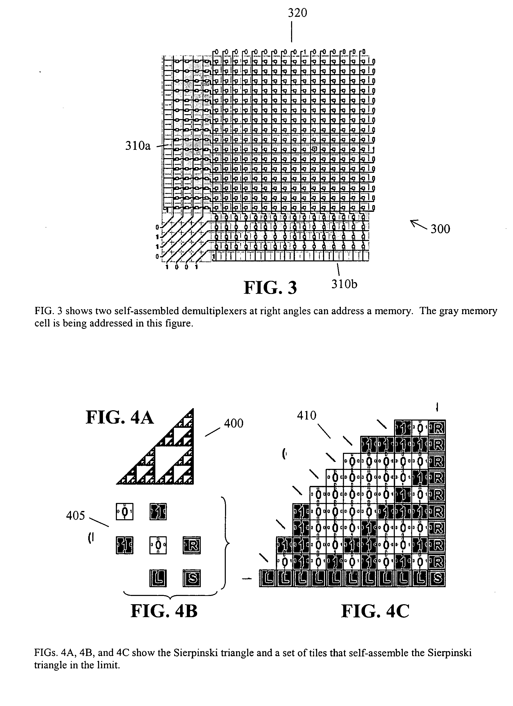
[0069] To illustrate certain principles and operations of the present invention, we have theoretically studied certain aspects of the invention defined herein and described aspect of this theoretical work below. As will be appreciated, this theoretical work is merely exemplary and should not unduly limit the scope of the claims herein. One of ordinary skill in the art would recognize many variations, modifications, and alternatives. Also, the theoretical examples described herein are merely intended to assist the reading in understanding certain aspects of the invention without limiting the claims as recited herein.

[0070] To expand on the same basic concepts introduced above, it is noted that self-assembly is a process in which basic units aggregate under attractive forces to form larger compound structures. Recent theoretical work has shown that pseudo-crystalline self-assembly can be algorithmic, in the sense that complex logic can be programmed into the growth process. This theo...


PUM

PropertyMeasurementUnit
assembling molecular structuresaaaaaaaaaa
attractive forcesaaaaaaaaaa
forcesaaaaaaaaaa

Abstract

A self-assembly method for circuit patterns includes generating a set of tiles, each of the tiles corresponding to a segment of molecules, the set of tiles comprising a set of rule tiles and a set of boundary tiles, each tile having one or more binding regions; assigning a label from a set of labels to each binding region; self interacting, with attractive forces, one or more of the tiles with one or more other tiles among the set of tiles; associating using selective interaction of at least one boundary tile from the set of boundary tiles with at least one rules tile from the set of rules tiles based upon at least a label from the one boundary tile and at label from the one rules tiles; and bonding at least one binding region of the one boundary tile with at least one binding region of the one rules tile.

Description

CROSS-REFERENCES TO RELATED APPLICATIONS [0001] This application claims priority to U.S. Provisional Patent Application No. 60 / 470,636, filed May 15, 2003, titled “Algorithmically Self-Assembled Circuits and Templates,” of Matthew M. Cook et al., and is hereby incorporated by reference herein in its entirety for all purposes.STATEMENT AS TO RIGHTS TO INVENTIONS MADE UNDER FEDERALLY SPONSORED RESEARCH OR DEVELOPMENT [0002] Work described herein has been supported, in part by the National Human Genome Research Institute (Grant No. P50 HG02370, Alpha Project), National Science Foundation Career Grant No. 0093486, DARPA BIOCOMP Contract F30602-01-2-0561, and NASA NRA2-37143. The United States Government may therefore have certain rights in the invention.BACKGROUND OF THE INVENTION [0003] The present invention relates to apparatus and techniques for the formation of patterns. More specifically the present invention relates to apparatus and techniques for the self-assembly of patterns for...

Claims


Application Information

Patent Timeline
Patent Type & Authority Applications(United States)
IPC IPC(8): C12QC12Q1/68H01L21/00
CPCB82Y10/00G06N3/002G06N3/123
Inventor COOK, MATTHEWROTHEMUND, PAULWINFREE, ERIK
Owner CALIFORNIA INST OF TECH
Why Eureka
Try Eureka