Working system for substrate
- Summary
- Abstract
- Description
- Claims
- Application Information
AI Technical Summary
Benefits of technology
Problems solved by technology
Method used
Image
Examples
first embodiment
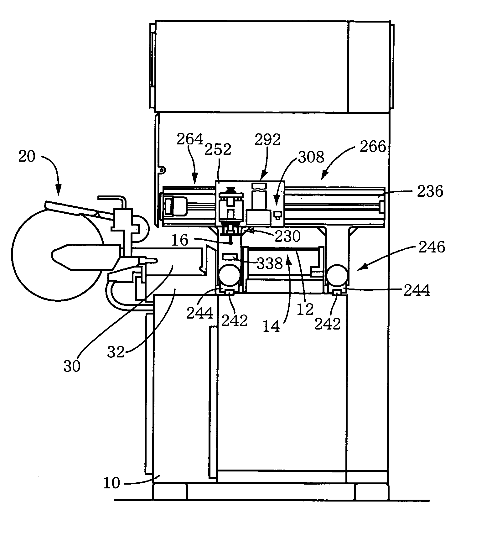
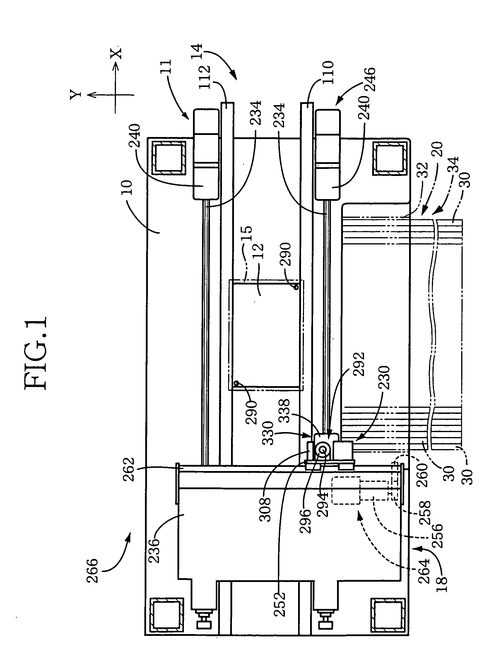
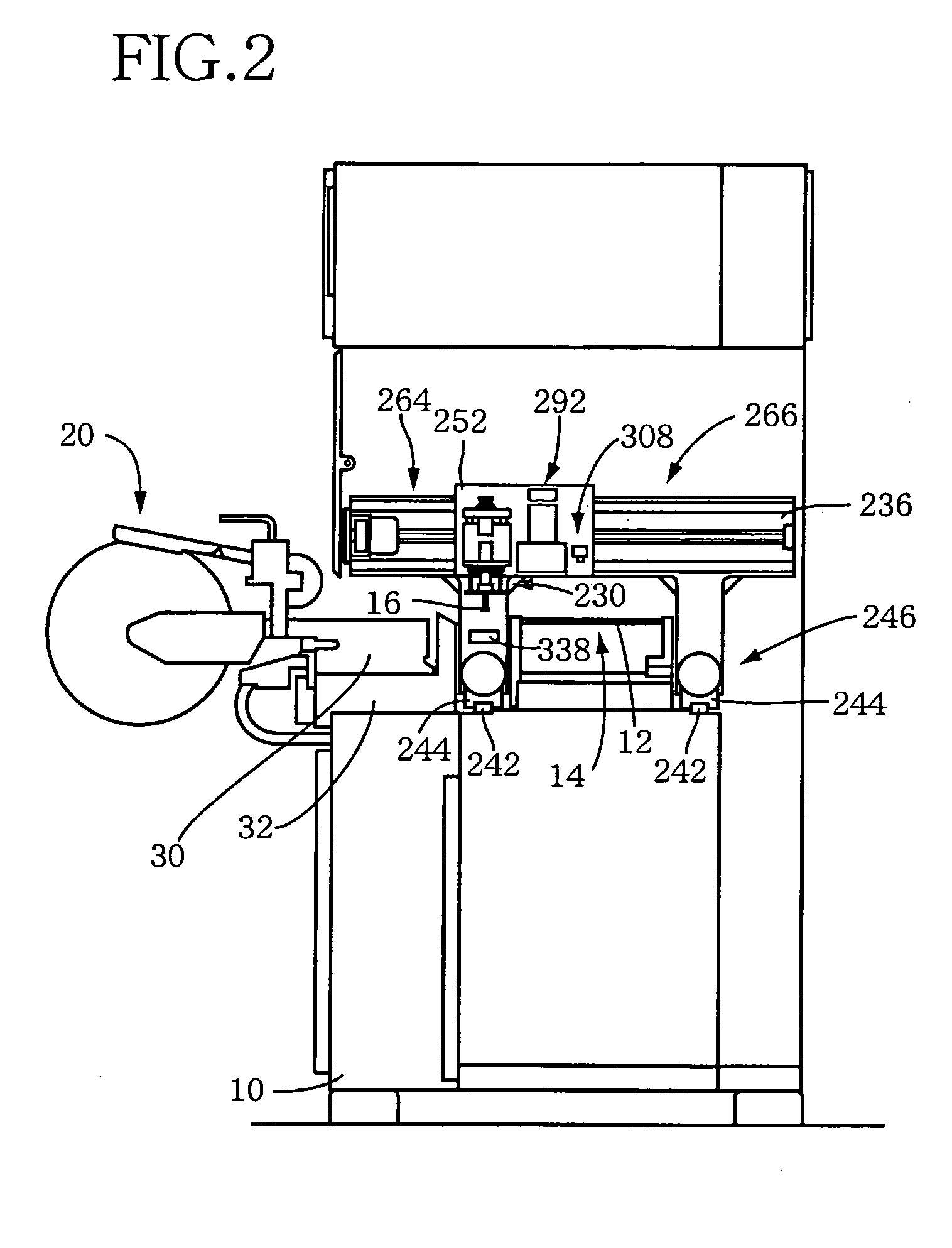
[0106] In this first embodiment, the electronic circuit components 16 supplied by the feeders 30 take the form of an electronic-circuit-component carrier tape accommodating a multiplicity of electronic circuit components arranged in a lengthwise direction of the tape at a predetermined pitch. The electronic-circuit-component carrier tape is accommodated in a tape accommodating device and fed by a tape feeder to feed the electronic circuit components 16 to the component supply portion. It is noted that the feeder may not be a tape feeder, but may be a bulk feeder which stores in bulk a number of electronic circuit components in a component-store device thereof, arranges the electronic circuit components into a single array, and supplies the electronic circuit components one by one from the component supply portion thereof by operation of a feeding device which uses vibration, an incline, airflow, conveyor belt or others, or a combination of some of these to feed the electronic circui...
second embodiment
[0162] In an electronic-circuit-component mounting system 400 a component imaging system 402 is disposed with its location fixed, at a position which is between a component supplying device 20 and a PWB conveyor 14, and which is a center position of a range of movement of a component mounting head 230 in the direction in which the PWB conveyor 14 conveys the PWB 12. That is, the component imaging system 402 is located at a position corresponding to a center position of a row of component supply portions of a plurality of feeders 30. The component imaging system 402 has a component camera 404 as an imaging device and a lighting device 406, is located below a plane of movement of the component mounting head 230, and operates to take a front elevational image and a projective image of an object.
[0163] When the PWB 12 is stopped at the center position in the conveying direction, an entirety of the PWB 12 is positioned in the vicinity of the component imaging system 402, thereby improvi...
third embodiment
[0165] In the embodiments described above, the predetermined detection portion of the PWB 12 is detected by the photoelectric sensors and then the PWB 12 is stopped. However, the detection may be implemented by taking an image with an imaging device, after which the PWB 12 is stopped. Such an embodiment (third embodiment) will be described by reference to FIGS. 16-18.
[0166] Except the control of stopping the PWB 12, an electronic-circuit-component mounting system 420 according to the third embodiment is constructed similarly to the electronic-circuit-component mounting system 11 as described above, and the similar part is not described here.
[0167] In the third embodiment, a fiducial-mark camera 294 of a fiducial-mark imaging system 292 takes an image of a downstream-side edge of a PWB 12 in a conveying direction so that the PWB 12 is detected, decelerated and stopped. That is, the imaging device for taking an image of a predetermined detection portion of the PWB 12 is adapted to ta...
PUM
| Property | Measurement | Unit |
|---|---|---|
| Shape | aaaaa | aaaaa |
| Dimension | aaaaa | aaaaa |
Abstract
Description
Claims
Application Information


