Shower head structure for processing semiconductor

a technology of semiconductor and shower head, applied in the direction of individual semiconductor device testing, semiconductor/solid-state device testing/measurement, instruments, etc., can solve the problem of deteriorating uniformity of film thickness over the wafer surface, a certain difference between the actual wafer temperature and the detected temperature, etc. problem, to achieve the effect of improving the uniformity of the intra-surfa

Inactive Publication Date: 2005-06-02
TOKYO ELECTRON LTD
View PDF4 Cites 51 Cited by
  • Summary
  • Abstract
  • Description
  • Claims
  • Application Information

AI Technical Summary

Benefits of technology

[0010] It is, therefore, a primary object of the present invention to provide a shower head structure and a semiconductor processing device and method that can improve an intra-surface uniformity in the processing of semiconductor even when a radiation thermometer being used.

Problems solved by technology

Hence, there inevitably occurs a certain difference between the actual wafer temperature and the detected temperature.
In case of using the radiation thermometer, if an extra thin film deposited on an incident plane of a light probe for collecting light emitted from the wafer, the wafer temperature cannot be measured accurately because the thin film absorbs the light.
As a result, a thickness of the film where the certain gas is provided is changed and the uniformity of film thickness over the wafer surface is deteriorated.
In this case, the wafer temperature cannot be measured accurately.

Method used


Image

  • Shower head structure for processing semiconductor
  • Shower head structure for processing semiconductor
  • Shower head structure for processing semiconductor

Examples


Embodiment Construction

[0041] Preferred embodiments in accordance with the present invention will now be described with reference to the accompanying drawings. Parts having substantially same functions and same structures will be designated with like reference numerals, and a description thereof will be repeated only when necessary.

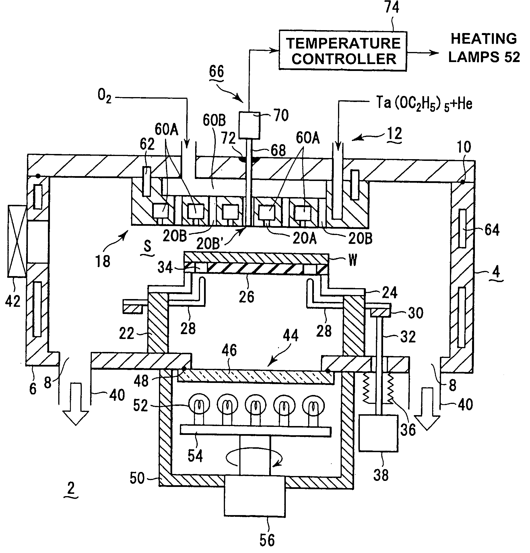
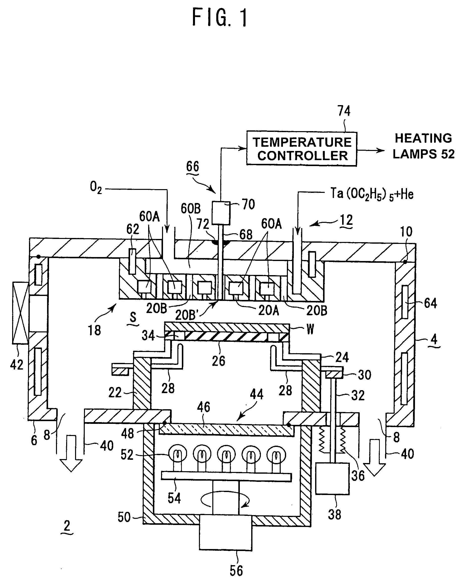
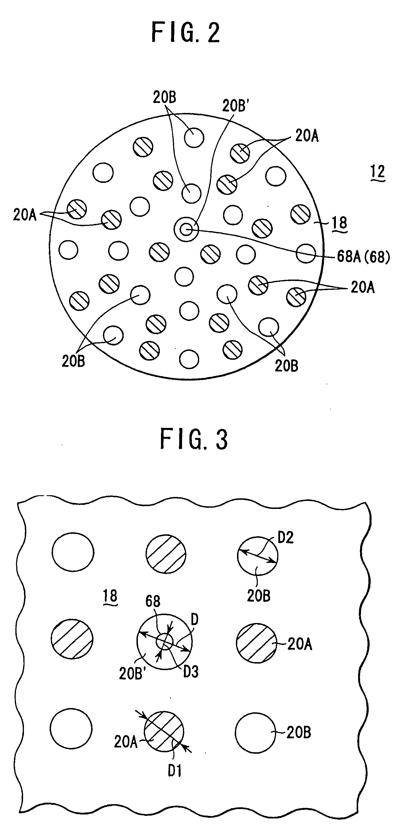
[0042]FIG. 1 presents a structural diagram showing a semiconductor processing device including a shower head structure in accordance with a preferred embodiment of the present invention. In this embodiment, a semiconductor processing will be exemplified by a case where a tantalum oxide film, i.e., a metal oxide film, is formed by CVD.

[0043] As shown in FIG. 1, a processing device 2 includes a processing chamber 4 formed in a shape of a cylinder, e.g., by using aluminum. Exhaust ports 8 are arranged at a bottom portion 6 of the processing chamber 4, which enables vacuum pumping in the processing chamber. A shower head 12 is installed at a ceiling of the processing chamber 4 th...


PUM

PropertyMeasurementUnit
temperatureaaaaaaaaaa
diameter D1aaaaaaaaaa

Abstract

A shower head structure disposed in a device 2 for processing a semiconductor while supplying processing gas to a processing space S for storing a heated processed substrate W, comprising a shower head 12 having a plurality of gas injection holes 20B for supplying the processing gas and a light introducing rod 68 of a radiation thermometer 66 inserted into at least one of the gas injection holes 20B.

Description

FIELD OF THE INVENTION [0001] The present invention relates to a shower head structure for semiconductor processing and a semiconductor processing device and method to execute processes of forming a metal oxide film, etching, and the like. The term semiconductor processing used herein denotes various processes executed so as to manufacture on a substrate a structure including semiconductor devices, and wiring and electrodes connected thereto by forming semiconductor layers, insulating layers, electrically conductive layers, and the like, on the substrate such as a semiconductor wafer and a LCD substrate. BACKGROUND OF THE INVENTION [0002] In case of manufacturing a semiconductor device, a film forming processing and a pattern etching processing are repeatedly carried out with respect to a semiconductor wafer. Specifications of the film forming processing become stricter every year as the semiconductor device becomes of a higher density and higher integrity. For example, such a very ...

Claims


Application Information

Patent Timeline
Patent Type & Authority Applications(United States)
IPC IPC(8): H01J37/32H01L21/00H01L21/3065H01L21/31C23C16/52
CPCH01J37/3244H01L21/67115H01J37/32935
Inventor TAKAGI, TOSHIOSAKUMA, TAKESHIKATO, YUJIMATSUMOTO, KENJI
Owner TOKYO ELECTRON LTD
Why Eureka
Try Eureka