Single type of semiconductor wafer cleaning apparatus and method of using the same

a cleaning apparatus and semiconductor technology, applied in the direction of cleaning process and apparatus, cleaning using liquids, chemistry apparatus and processes, etc., can solve the problems of low production efficiency, low cleaning efficacy, and high cleaning efficacy, and achieve high concentration of ozone, simple structure, and high degree of efficacy

Inactive Publication Date: 2005-06-09
SAMSUNG ELECTRONICS CO LTD
View PDF5 Cites 7 Cited by
  • Summary
  • Abstract
  • Description
  • Claims
  • Application Information

AI Technical Summary

Benefits of technology

[0007] An object of the present invention is to overcome the problems, disadvantages and limitations of the prior art. More specifically, it is a first object of the present invention to provide a single type of semiconductor wafer cleaning apparatus having a simple structure, capable of producing a cleaning solution having a high concentration of ozone (O3), and capable of producing other various cleaning solutions. It is likewise a second object of the present invention to provide a method of cleaning a semiconductor wafer with a high degree of efficacy.

Problems solved by technology

Although the production efficiency of the batch type of semiconductor cleaning apparatus is high, the cleaning efficacy is low.
On the contrary, in the single type of semiconductor wafer cleaning apparatus, the production efficiency is low, and the cleaning efficacy is high.
Thus, it is difficult to use ozone (O3) in high concentrations and at high temperatures in a bath type of semiconductor wafer cleaning apparatus.

Method used


Image

  • Single type of semiconductor wafer cleaning apparatus and method of using the same
  • Single type of semiconductor wafer cleaning apparatus and method of using the same
  • Single type of semiconductor wafer cleaning apparatus and method of using the same

Examples


Embodiment Construction

[0020] The present invention will be described more fully with reference to the accompanying drawings.

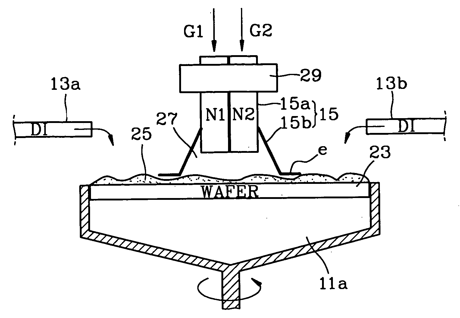
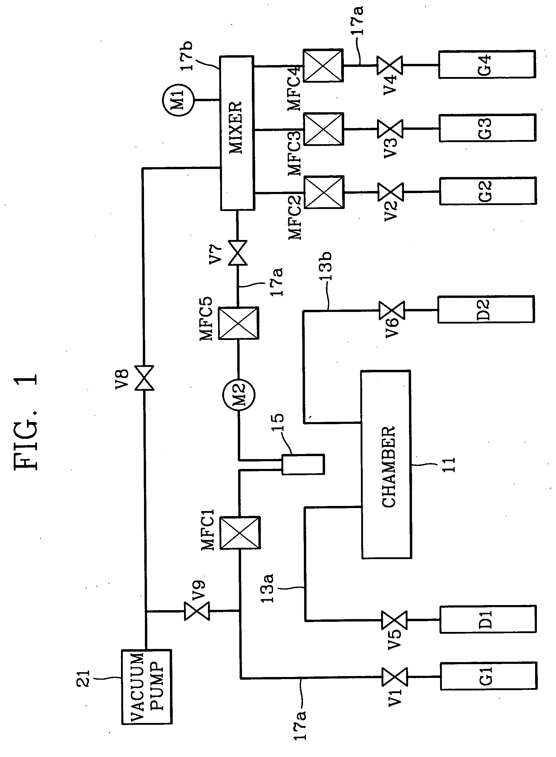
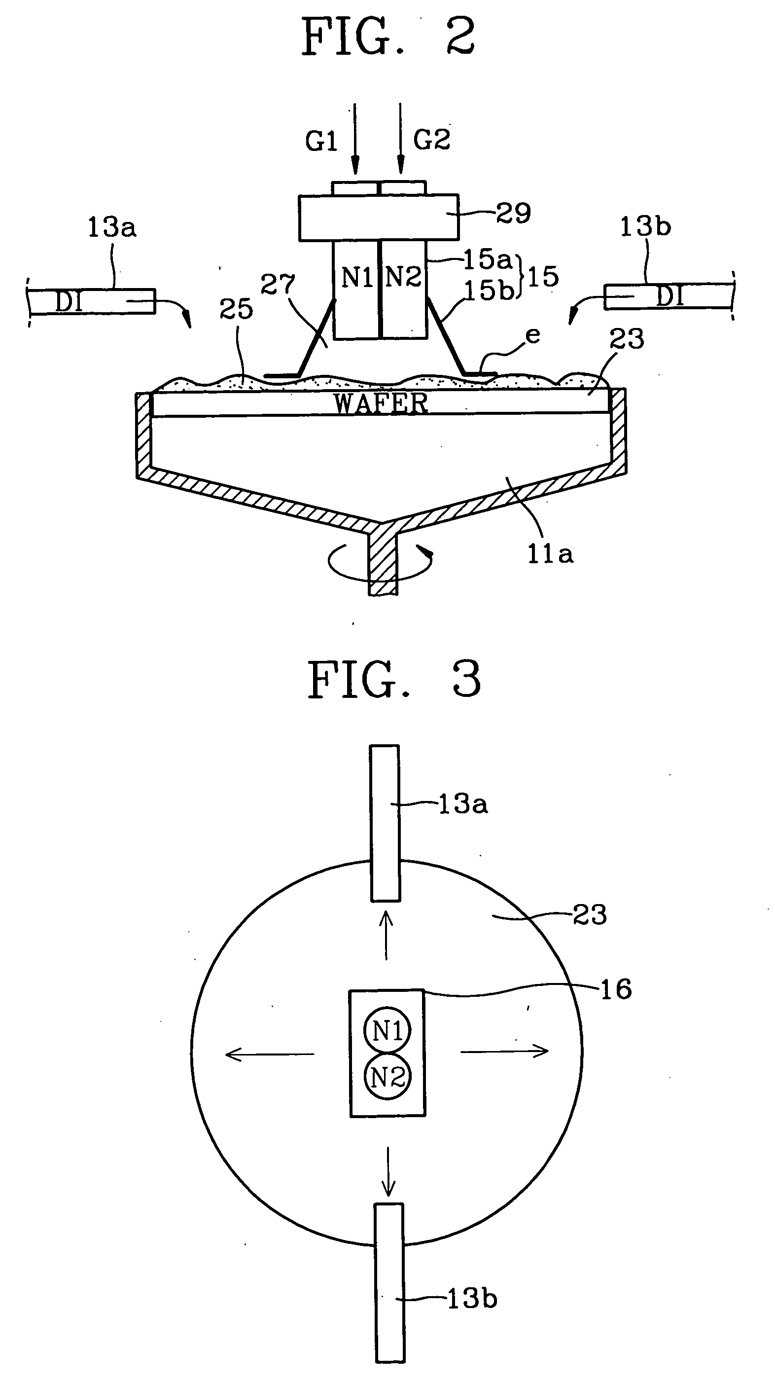
[0021] Referring now to FIGS. 1 and 2, a single type of semiconductor wafer cleaning apparatus according to the present invention includes a chamber 11 into which a wafer 23 is loaded, a rotatable chuck 11a disposed in the chamber 11 and to which the wafer 23 is mounted, and a de-ionized water supplying means for supplying de-ionized water onto the wafer from the side(s) of the chamber 11. The de-ionized water supplying means includes de-ionized water supply sources D1 and D2, valves V5 and V6, and at least one and preferably, two or more, de-ionized water supply lines 13a and 13b.

[0022] The semiconductor wafer apparatus also includes a gas spraying unit 15 for spraying gas towards the wafer, and a gas supply means for supplying gases to the gas spraying unit 15. The gas supply means includes gas supply sources G, a gas line 17a, valves V1 through V4 and V7 through V9, mass flow c...


PUM

PropertyMeasurementUnit
distanceaaaaaaaaaa
pressureaaaaaaaaaa
internal pressureaaaaaaaaaa

Abstract

A semiconductor wafer cleaning apparatus includes a gas spraying unit, having a gas injection tube and a gas guard extending therearound, for spraying cleaning gas into a water layer formed on a wafer. The gas guard forms a small chamber just above the water layer, so that the partial pressure of gas injected from the gas injection tube is increased in the small chamber, whereupon the cleaning gas readily dissolves in the water layer. As a result, a cleaning solution having a high concentration of cleaning gas is produced, whereby the cleaning efficacy of the solution is high. Subsequently, a drying gas, such as isopropyl alcohol, for drying the wafer can be ejected onto the water layer using the gas spraying unit. Thus, the semiconductor wafer cleaning apparatus has a simple structure.

Description

BACKGROUND OF THE INVENTION [0001] 1. Field of the Invention [0002] The present invention relates to a semiconductor wafer cleaning apparatus. More particularly, the present invention relates to a single type of semiconductor wafer cleaning apparatus and to a method of cleaning a semiconductor wafer using the same. [0003] 2. Description of the Related Art [0004] In general, semiconductor wafer cleaning apparatuses include batch and single types. In the batch type of semiconductor wafer cleaning apparatus, several semiconductor wafers are cleaned simultaneously. Although the production efficiency of the batch type of semiconductor cleaning apparatus is high, the cleaning efficacy is low. On the contrary, in the single type of semiconductor wafer cleaning apparatus, the production efficiency is low, and the cleaning efficacy is high. When manufacturing highly-integrated semiconductor devices it is important that the semiconductor wafer be very clean at several stages in the process. T...

Claims


Application Information

Patent Timeline
Patent Type & Authority Applications(United States)
IPC IPC(8): B08B3/08B08B5/00B08B3/12H01L21/304
CPCB08B3/08Y10S134/902B08B3/12H01L21/304
Inventor LEE, KUN-TACKHAN, YONG-PILHAH, SANG-ROK
Owner SAMSUNG ELECTRONICS CO LTD
Why Eureka
Try Eureka