Electric field sensor
Inactive Publication Date: 2005-06-09
BAE SYST INFORMATION & ELECTRONICS SYST INTERGRATION INC
40 Cites 53 Cited by
AI-Extracted Technical Summary
Problems solved by technology
It is low cost, passive, low power, long life, and extremely small.
However, unlike visual, infra-red, audio, and other spectra detected using prior art sensors, there are no presently kn...
View moreBenefits of technology
[0022] Embodiments of the present invention are included herein, wherein the present invention is designed in contemplation of the deficiencies of the prior art. The present invention is an E-field detector system including at least one E-field distortion sensor that can detect distortion of the E-field by a person, vehicle, weapon, or electric power source. The present invent...
View moreAbstract
The invention is a detection system comprising inexpensive, miniaturized sensors for detecting electric field (E-field) disturbances. Such sensors are easily and covertly deployable and have low power consumption. The devices may incorporate visual or audio alerts and can include communications hardware for transmitting data for further processing of the electrostatic events.
Application Domain
Technology Topic
Image
Examples
- Experimental program(1)
Example
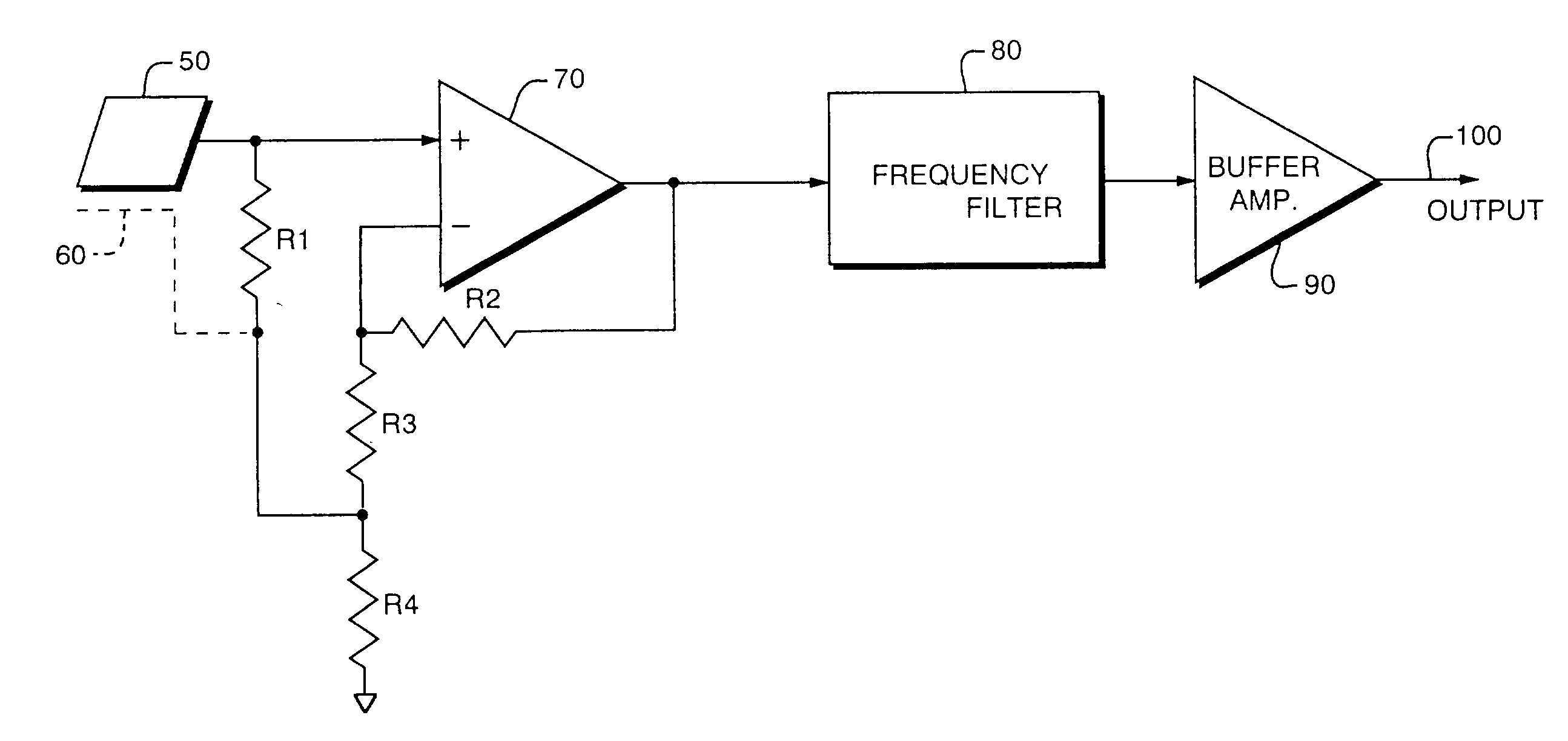
[0053] To those skilled in the art, the invention admits of many variations. The following is a description of a preferred embodiment, offered as illustrative of the invention but not restrictive of the scope of the invention. Electro static event (ESE) sensors and systems according to the present invention exploit unintended and unavoidable electrostatic emissions in the spectrum from sub 1 Hz to greater than 1 MHz. The sensors are passive, low cost, small, low power and examine unintended or unavoidable emissions.
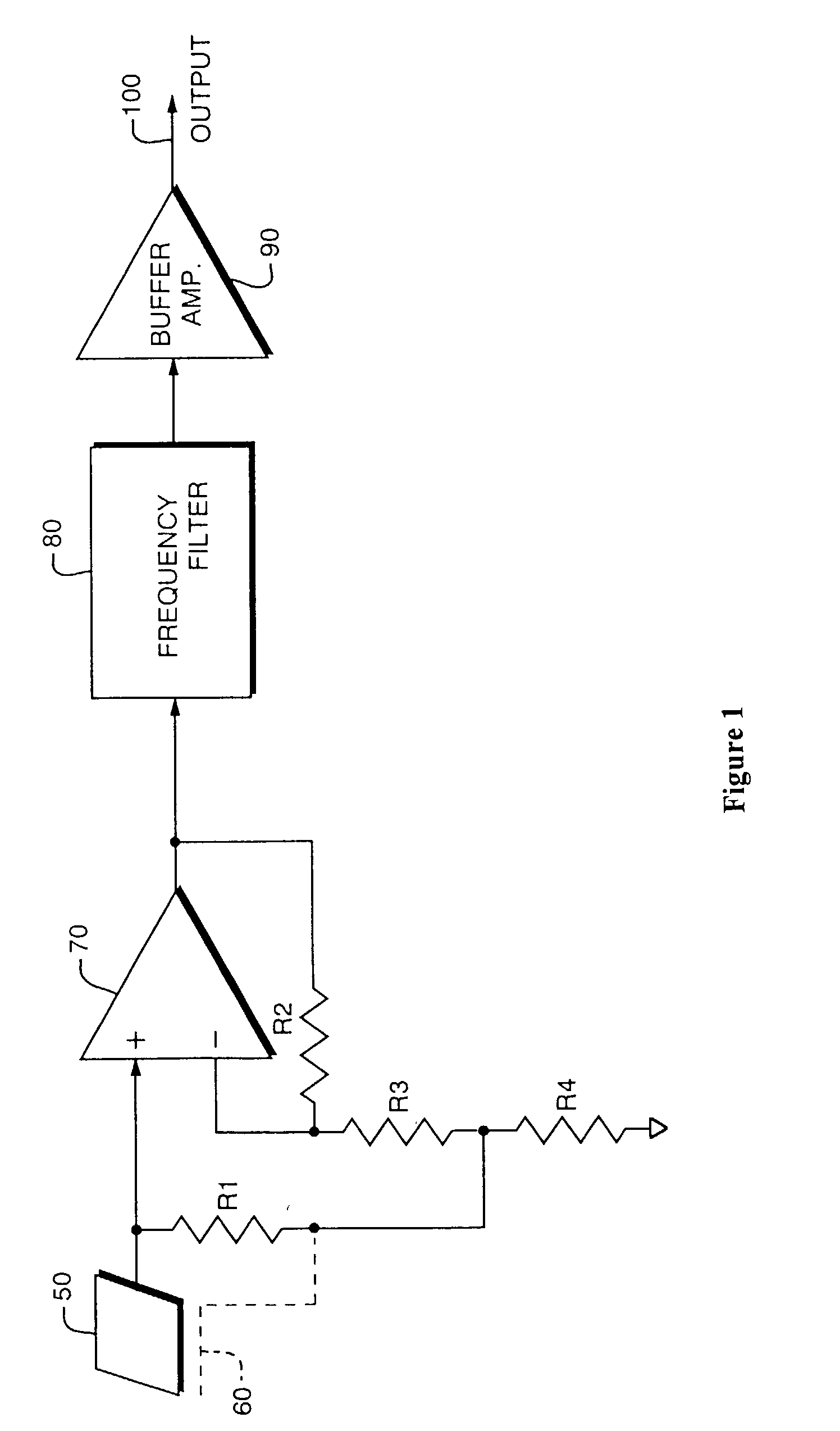
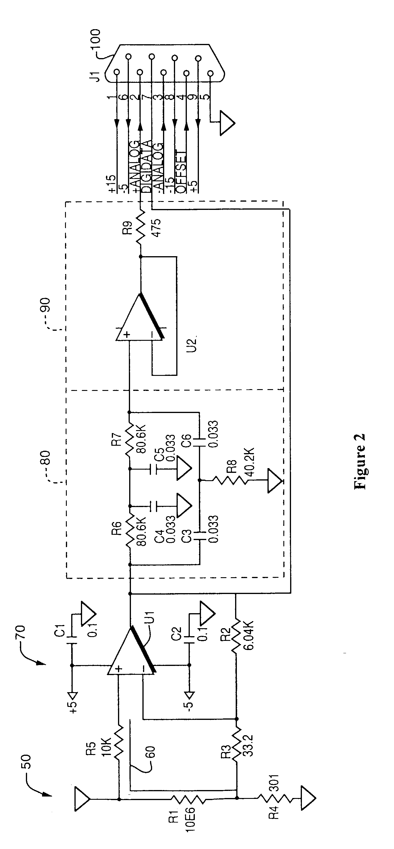
[0054]FIG. 1 is a block diagram representing a simple embodiment of the present invention sensor for detecting E-field distortions illustrating the circuit arrangement as well as the interconnection of the inputs and outputs. The sensing area 50 or “antenna” is generally a small receptive element, and in a preferred embodiment the sensing area 50 is a printed wiring board (PWB) etch or pad although it could also be an external sphere or other receptive unit.
[0055] The sensor area 50 in FIG. 1 can essentially be regarded as one side of a capacitor with the other side being the charged source or even the earth's field being the source. The larger the area the greater the sensitivity, however interference and extraneous signals become problematic if the reception is too high. In one embodiment the pad is approximately {fraction (1/30)} inch and picks up signals as low as 200 millivolts. Experimentation of other sensing areas from about {fraction (1/10)} of a square inch to several inches has resulted in different data measurements and the size of the antenna depends upon the application and environmental conditions.
[0056] There is a guard area 60 proximate the sensing element which functions to reduce the ‘capacitance’. In one embodiment where the circuit is laid out on a printed circuit board, the guard area is a wiring board etch on the opposite side of printed circuit board opposing the sensing area 50. The guard 60 primarily eliminates the capacitance of the shield, such as coax cable, thereby greatly increasing the antenna 50 impedance. The sensing area 50 does not need to be a large area sensing element, as experimentation revealed that large sensing elements picked up too many extraneous signals to be useful. In one embodiment the sensing element 50 is designed for maximum input impedance with a partial Faraday shield (not shield) covering a portion of the sensing area 50 to reduce the gain.
[0057] Thus, the size of the sensor area 50 is one method to adjust system gain, while another adjustment mechanism is the shielding. Subsequent signal processing and filtering is used to reject unwanted signals, for example, narrow pulses or relatively high frequency signals such as those caused by lightening, arc welders, and RF sources are rejected. It should be noted that a typical signal response in the range of 0.1-5 kHz does not have any DC bias.
[0058] The differential amplifier 70 is used with bootstrapping to establish high impedance and provide amplification. The gain of the differential amplifier 70 is determined by the resistors R2, R3, and R4 and as is well known in the art, that the gain is equal to (R2+R3+R4)/(R3+R4). The resistors R3 and R4 determine the percentage of input signal that is coupled to one side of R1 and the guard 60. For example, R3=1 k and R4=9 k, the voltage at the junction of R3 and R4 is 90% of the voltage at the sensing area 50. In effect, R1 appears ten times larger, and the capacitance of the sensing area 50 to be ten times lower.
[0059] Expressed differently, if the voltage at the junction were 99.9% of that present at the sensing area 50, the R3 would appear 1000 times larger and the capacitance of the sensing area 50 would appear to be 1000 times smaller. Thus the ratio of R3 to R4 determines the input resistance to the amplifier 70. It is preferred to make the input impedance very high without having amplifier 70 saturate due to its input bias currents. Typical feedback ratios are from 90% to 99% while the value of R1 might be 10 Mohms, giving an effective input resistance of 100 to 1000 Mohms or more.
[0060] In a preferred embodiment, the differential amplifier 70 is a field-effect operational amplifier U1 (op amp TLC2272) with bootstrapping to provide high impedance for the sensing element 50. In this circuit, the sensing element 50 is a small metallic piece that is part of the printed wiring board, such as an etch on the board. The sensing element signal is amplified and converted to a low source impedance. R1 is 10 Mohm, R2 is 6.04 Kohm, R3 is 33.2 ohm and R4 is 301 ohm. An additional resistor R5 may be connected between the sensing area 50 and the + input of the differential amplifier 70 of approximately 10 Kohm to provide amplifier protection.
[0061] A frequency filter 80 is used to isolate the signals of interest. A power line frequency notch filter 80 is used to reject the E field caused by power lines and is set to the power line frequency for the region of use, generally 60 Hz in the United States. In one embodiment, off-the-shelf commercial components are utilized to construct the filter 80. The 60 Hz notch filter 80 is inserted to reject power line and minimizes the chance of saturation of the next amplifier stage for the 60 Hz noise. Other filters may also be used depending upon the operating environment, such as differing noise parameters for 50 Hz and 400 Hz electrical environments. Those skilled in the art are familiar with the appropriate resistor and capacitor arrangement necessary to produce the notch filter 80.
[0062] Other filters include bandpass, highpass and lowpass filters that are used in certain circumstances. In one embodiment the invention is intended to detect the 60 Hz power lines, and a bandpass filter about 60 Hz is used. In other embodiments the 60 Hz noise has interfering signals such that commutating or digital signal processor filtering is required to select a smaller bandwidth for detection.
[0063] The buffer amplifier 90 provides high input impedance to the filter 80 while providing additional gain and a low impedance source for the voltage measuring device. Typically the measuring device is a sample-and-hold circuit followed by an analog-to-digital (A/D) converter and subsequent processing circuitry.
[0064] The buffer amplifier stage 90 in one embodiment is a second field-effect operational amplifier U2 (op amp TLC2272) and is used to achieve an approximate gain of 20 dB. A 15 v DC power is supplied by a power source, such as common dry cell batteries, although any power source with acceptable output may be used. The output signal of the sensor device is delivered to the next stage of the detection system.
[0065] The sensor does not require unique components and persons skilled in the art will choose components that will enable optimal configuration to achieve the objectives of the sensor's application. The combination of the sensing elements and guard in conjunction with the bootstrapped differential amplifier and other elements enables the unexpected sensing of electric field disturbances in a wide array of applications.
[0066]FIG. 2 is a schematic of one circuit illustrating the component selection for the differential amplifier as well as the electrical interconnection. In this embodiment an off-the-shelf commercial components are utilized. A field-effect operational amplifier (op amp) U1 such as TLC2272 is used to perform impedance matching for the sensing antenna 50. In this circuit, the sensing antenna 50 is a small metal pad on a printed circuit board with a corresponding guard 60 on the opposite side of the board. The effective antenna impedance is approximately 1000 Mohms and the sensing area signal is amplified to a low (≅50 ohms) source by the amplifier U1. The bootstrapping interface discussed herein establishes the high impedance input and provides amplification.
[0067] A 60 Hz notch filter 80 is inserted to reject power line and signal noise and minimizes the chance of saturation of the final amplifier stage 90. The selection of components R6, R7, R8, C3 and C6 are selected as known in the art and other values are possible. There may also be operating environments where other frequency ranges are excessive, such as 50 Hz and 400 Hz, and the notch filter(s) are designed to eliminate the most detrimental interference.
[0068] The second field-effect operational amplifier (op amp) U2 is used to achieve an approximate gain of 20 dB. DC power is supplied by common dry cell batteries in one embodiment, however power can also be provided from an AC source after AC/DC conversion. Other power sources such as solar and coupling power from power lines have also been contemplated. The sensor device output signals are delivered to the next stage of the detection system (not shown) through a connector J1.
[0069]FIG. 3 shows one embodiment that encompasses dual sensors 300 for a differential field sensor and the signal processing requirements. It should be understood that the device can be run in single ended mode by grounding one antenna 300 which can allow for redundancy. The parallel connections allow the processing unit 390 to gather data from the multiple sensors 300 and process the data accordingly.
[0070] This embodiment employs two sensing elements 300 and two corresponding bootstrapped preamps 310 for boosting the input signal strength. The output of the preamps 310 are connected to a differential amplifier 320 and 60 Hz notch filter 340. The notch filter 340 can also be bypassed by switch SW1. A programmable filter 350 and programmable gain stage 360, and logarithmic amplifier 370 (logamp) are employed to process and enhance the electrostatic signature of the detected source prior to its passage to the analog and digital converters 380 generating digital data representing the received signals. The digitized data is coupled to a processing unit 390 such as a microprocessor or microcontroller which performs processing to configure the output signal parameters for use by the next stage of the detection system. An optional Digital-to-Analog converter 400 can be used to re-convert the digitized data to analog form in order to have the raw data presented to the user.
[0071] In this embodiment the programmable filter 350 includes an Allpass, Bandpass, Highpass and Lowpass filtering depending upon the application. The selectability of filtering via switch SW3 allows flexibility in isolating the electrostatic field being analyzed as well as eliminating interfering noise. The programmable gain stage 360 permits variable boosting of the received signal. The log amp 370 boosts the signal depending upon the input level to a level satisfactory for further processing. In this embodiment the log amp stage 370 can be bypassed by switch SW2. The control to the programmable filter 350 and gain stage 360 are commands from the local signal processor although external commands via hard wired or wireless are within the scope of the invention. The output of the differential field sensor is delivered to the next stage of the detection system at the output terminal.
[0072] In one embodiment, the processing unit 390 has internal memory (not shown) or connection to external memory that stores the measured data or counter information. The counter data can track the number of times the threshold level was reached indicating, for example, the number of vehicles passing a toll or down a street. The output data can also be stored to establish a library of E field signatures that allow for classification and identification of measurements. This stored data is useful when comparing the present measurements to the existing database. For example, the signature of a certain ballistic can possibly be matched for future measurements.
[0073]FIG. 4 illustrates one embodiment for an E field unit 400 encompassing various supporting functionality. The sensing elements 410 provide the E field measured data to the analog sensors 420 that filter and amplify the signals as described herein. The analog output from the sensors 420. The dual sensors 420 can be used singularly and allow for redundancy and switch from a faulty sensor to a working sensor. Alternatively, the dual sensors can take data in different axes or otherwise supplement the measurement information. Multiple sensor measurements aid in coherent processing as described herein. The entire unit can be encased in a housing 415 to provide protection from the elements.
[0074] The analog output of the processing electronics 420 is delivered to an event detector 430 that is preset to a certain voltage level in order to wake up the microprocessor 450 once a certain level is detected. The term microprocessor, microcontroller and processing unit are used interchangeably to denote a processing section and associated elements such as timing and memory. In one embodiment, the sensing unit 400 processes the information internally and stores the data until a certain threshold level is detected, a time interval elapsed, a count number is attained or an instruction is received before transmitting date externally. The event detector 430 allows elements of the unit 400 to consume lower power levels until a threshold level is attained or for batched transmission of data. The output of the processing electronics 420 also connects to an analog-to-digital (A/D) converter 440 that converts the analog voltage signal to a digitized form.
[0075] The microcontroller 450 is the control center for the unit 400 and controls the subsequent processing once an event is detected. In a first embodiment a global position system (GPS) module 470 is coupled to the microcontroller 450 in order to establish an extremely accurate standard time reference as well as geographic location. Other types of clock references are also within the scope of the invention such as internal local oscillators. The microcontroller 450 uses the position information and timing data to determine the location of the unit and time of the measured event.
[0076] The microcontroller 450 is also coupled to a datalink 460 such as a cellular modem module that is a low power RF link to the outside world and allows the unit 400 to transmit and receive data. The data link 460 transmits the measured data as well as receives instructions or commands from a central host. For power savings the unit can batch measurements for periodic transmission or only transmit signals upon the occurrence of certain events. There are additional elements sometimes associated with the microcontroller 450 to provide random access memory (RAM) and flash memory as well as timing. The datalink 460 is a single example of the wireless connectivity available to communicate with a central host or other units. The communications can also incorporate RFID technology whereby the data is only transmitted once a signal triggers the transceiver. Hardwired communications is also a viable implementation depending upon the application, and an external interface couples to the appropriate interface card. Optional components include audible and visual indicators (not shown) that would generate alerts once an event is detected.
[0077] The power source for the unit 400 is derived from several possible sources. There can be an external power supply connected to the external connection 530 that provides the power directly or through a transformer unit (not shown). In the illustrated embodiment the power source is DC storage cell 510 supplying a 3.3V DC or 12V DC. A battery 510 may be the sole source of power, and coupled to the power distribution section 500 that redirects the power and encompasses appropriate filtering and fuse protection. A solar cell 520 can be used to operate the unit 400 and also provide a power source that can charge the battery 510 and extend the life span of the unit 400. In one implementation, the unit is coupled to power lines and draws power from the high tension lines. As should be appreciated the supplemental components are applications specific and the cost, weight, size, power are some of the factors that contribute to the specific embodiment for a particular application.
[0078] The solar cell power 520 is most practical to those implementations wherein the unit is mounted to a structure for extended periods of sensing. For example, a perimeter security system that places a plurality of units around a house or site can secure the sensors to fence posts of other structures that allow sunlight to charge the unit.
[0079] One feature of the present invention is a built-in-test capability. A metal rod or conducting strip (not shown) on the printed circuit board can be charged by coupling to the power source, wherein the sensor picks up the signal energy and tests the functionality.
[0080] As noted herein, the present invention detects the E field distortion of moving objects. Across the entire globe there is an atmospheric potential gradient (electric field) of approximately 200 V/meter of altitude. Research indicates that the natural electric field is geographically consistent, with the exception of atmospheric anomalies such as localized thunderstorms.
[0081] Changes in the state of presence, such as by walking as opposed to standing still, distorts the iso-potential lines. The individual footsteps and positioning is quantifiable via the sensor data. Similarly, high-voltage sources, static generators, and ionization have been found to create detectable electrostatic distortions. Connecting the E-field sensor of the present invention to a common oscilloscope and trace recorder enables detection and visual indication of a person walking past the sensors. Further, the detection and display of individual footsteps in the sensor's vicinity is also enabled, as is shown by the traces.
[0082] Referring to FIGS. 5a and 5b the electric field distortions created by a moving object in the E-field are illustrated. The sensors detect the distortion, d|E|/dt, created as a person moves through the electric field gradient of the atmosphere. Using the d|E|/dt sensors eliminates drift problems and allows detection of small “AC” changes in large “DC” fields. It also allows some measurements such as closest approach to be a zero crossing detect as opposed to an estimate of the maximum.
[0083] Referring to the test results of FIG. 5a, a single sensor was deployed and a person walked nearby the detector as measured by a DC coupled oscilloscope. The E field axis uses millivolts as the unit and the time axis is in milliseconds. As depicted, the distortion created by the walking person caused a noticeable measurement several hundreds of millivolts about the noise floor which is about 160 millivolts. The point of closest approach is seen as the nearly vertical line at or about 4141 milliseconds. This distortion is easily detected and depends upon a number of factors including the size of the sensing element, the amount of amplification, the filtering, as well as the size of the object making the distortion and the distance from the object to the sensor. In one embodiment, the detection range was approximately 20-25 meters indicating that the device would be an excellent motion sensor for inside/outside a home as well as for military applications. Thus as a motion sensor, the E field detectors can detect movement of persons and objects and there is no practical circumvention.
[0084]FIG. 5b represents test results from a truck passing nearby a motion sensor unit, wherein this motion sensor unit was actually dual differential detectors employed in a crossed ‘X’ shape pattern. The use of multiple sensors and multiple axis observations enhances measurement capability by permitting coherent processing and providing an additional set of information. For example, the bearing or direction of the moving object can be ascertained by examining the multi-axes data. Each sensor has an applicable noise floor or base level and the E field distortion is reflected by the marked increase in the voltage levels.
[0085] As noted herein, the E field sensor of the present invention can be incorporated with other sensors types and integrated into existing sensor designs. For example, the ground sensor of FIG. 6 is a low power, miniature intemetted unattended sensor 600 intended for battlefield deployment. The sensor can be deployed by hand, projectiles, mortars, missiles and aircraft. In this embodiment, there is a rotating camera 610 providing a visual feed. There are several acoustic sensors 620 to pick up various communications for intelligence gathering. At the end of each of the four sensor rods are the sensing elements 630 for the E field detection. A coaxial cable 640 connects from the sensing element 630 to the internal processing section 670 wherein the bootstrapped dual differential amplifier, filter and amplification stages are encompassed within the unit 600. There are also magnetic sensors 660 and seismic sensors 690 that enable comprehensive intelligence gathering and tracking capabilities with everything encased in a sturdy housing 695. The information from the various sensors is processed by the processing section 670 and is relayed to one or more central locations for further processing. In one embodiment the unit is powered by a battery although other power forms are within the scope of the invention. A plurality of units can be deployed to aid in battle strategies and the interconnected sensors cooperate to cover large areas.
[0086] Another important application of the present invention is related to inclusion on various deployable sensing systems, such as payloads. The E field sensors are valuable improvements that can be used with or without pods. During battle deployment, aerial sensor types can be deployed by various systems such as parachute, UAV, gliders, and various other airborne vehicles. The sensors typically include imaging systems, GPS/altimeter, data link, sensors and a power source. The cost, size, weight, power consumption of the E field sensors allows incorporation into these devices. And, the sensors contribute to the capability to detect the location of enemy fire and aid in directing a response. The sensors can also help to enhance overall survivability of the UAV's and other airborne sensing devices by providing advance information of threats.
[0087] Referring to FIGS. 7a-7e, the E field distortion associated with power lines is described. In one embodiment, dual spectrum electric field (E) and magnetic field (H) sensors are developed by dual differential sensors using four sensors located at the ends of extended arms as represented by FIG. 7a.
[0088] In the power line embodiment, the sensors are measuring the 60 Hz signals, so a bandpass filter would be used to isolate the 60 Hz signals. FIGS. 7b-7e show test results as the E field sensor approaches the high voltage power lines. The 60 Hz amplitude and phase coherence increases and is easily discernable.
[0089] Thus, one embodiment of the present invention is a high power detector that can be used on airplanes and other airborne objects and vessels to alert the operator to potential hazards. In one test, the flow of electricity through the power lines is detectable greater than 50 feet from the lines. A unit can be integrated into the existing helicopter electronics or made as a separate unit. In either case, the E field sensing would cause an alarm, audible and /or visual, to alert the operator once a threshold level is reached.
[0090] Of particular importance is a warning system for helicopters. There are numerous helicopter crashes each year related to helicopters striking power lines. Helicopter blades in rotation have been noted to create appreciable interference that saturates the amplifiers within the 60 Hz region of a bandpass filter. In the helicopter embodiment, bandpass filters may not provide adequate filtering and DSP or commutating filtering that narrows the bandwidth can be used, wherein such filters are known in the art.
[0091] Another implementation is a safety warning device for utility personnel to indicate power on the lines, especially when the shorting system used by operators is not in place. There are various situations where power feeds the power lines from generators that are connected to the lines and the present device allows an inexpensive alerting device.
[0092] Although the dual spectrum measurements from the X and Y axis of the sensor of FIG. 7a are not necessary, additional data from the measurements may be used to detect and classify the load types such as resistive, inductive and motors with solid state controllers as well as the relative magnitudes. The sensors also detect the imbalances when loads are applied and removed and the events occurring on a grid. The leakage from the high tension lines can also be used to power the sensor.
[0093] As discussed herein, coherent processing from multiple sensors of a single measurement greatly improves the measurement capabilities by reducing the impact of noise and interference. The coherent processing is described in detail in related application U.S. application Ser. No. 10/256812, filed Sep. 27, 2002 which is incorporated by reference.
[0094] The coherent noise reduction works because the background noise is “far field” and low frequency. This means that two sensors placed apart see exactly the same background noise. If the signal of interest is in the near field, (less than 100 feet in one test) the sensors see the signal of interest at different signal strengths. When the two sensors are subtracted, the background noise disappears while some of the signal of interest remains. No knowledge of the background noise is required. This technology is well known to those skilled in the art and is applied to noise reduction head sets and microphones. This is distinguishable from bandpass filters, low pass filters, and high pass filters, that essentially reject interfering signals within a certain frequency. Bandpass filters reject signals in a certain frequency band. High pass filters reject lower frequency signals while allowing higher frequency signals. Low pass filters allow certain lower frequency signals while rejecting high frequency signals.
[0095] The noise reduction processing can be shown by the following equations for two sensors: [0096] S1(t) is the total signal received at sensor 1 [0097] S2(t) is the total signal received at sensor 2 [0098] P1(t) is the signal at S1 from the signal of interest [0099] Nb(t) is the background noise (assumed to be far field and therefore the same at both sensors) [0100] P2(t) is the signal at S2 from the signal of interest
S1(t)=Nb(t)+P1(t)
S2(t)=Nb(t)+P2(t)
P2(t)=kP1(t)
K<1
Sdiff=S1(t)−S2(t)=(Nb(t)+P1(t))−(Nb(t)+P2(t))
Sdiff=P1(t)−kP2(t)
Sdiff=(1−k)P1(t)
[0101] The signal of interest is somewhat reduced in strength but background noise is essentially eliminated. Thus signal to noise ratio (SNR) is greatly improved.
[0102] The inventors anticipate that persons skilled in the art can apply the coherent processing outputs of the present invention to analysis of the detected E-field disturbance such that the particular source of the E-field disturbance can be detected at useful distances and distinguished from other E-field disturbance and noise sources in the vicinity.
[0103] The objects and advantages of the invention may be further realized and attained by means of the instrumentalities and combinations particularly pointed out in the appended claims. Accordingly, the drawing and description are to be regarded as illustrative in nature, and not as restrictive
[0104] The foregoing description of the embodiments of the invention has been presented for the purposes of illustration and description. It is not intended to be exhaustive or to limit the invention to the precise form disclosed. Many modifications and variations are possible in light of this disclosure. It is intended that the scope of the invention be limited not by this detailed description, but rather by the claims appended hereto.
Login to view more PUM


Description & Claims & Application Information
We can also present the details of the Description, Claims and Application information to help users get a comprehensive understanding of the technical details of the patent, such as background art, summary of invention, brief description of drawings, description of embodiments, and other original content. On the other hand, users can also determine the specific scope of protection of the technology through the list of claims; as well as understand the changes in the life cycle of the technology with the presentation of the patent timeline. Login to view more.
Login to view more Similar technology patents
Electronic scale
InactiveCN104838243AAvoid damageLow costWeighing apparatus using elastically-deformable membersSpecial purpose weighing apparatusMechanical engineering
Owner:SUZHOU VOCATIONAL UNIV
Thin walled, two component cartridge casing
Owner:TECH CORPORATION CO LTD
Power over Ethernet-prioritized active splitter
ActiveUS20050229016A1Low costLong period of timeMechanical power/torque controlDc network circuit arrangementsPower over EthernetSafe system
Owner:ADEMCO INC
Thin-film transistor fabrication process and display device
InactiveUS20100044701A1Low costEasy to manufactureSolid-state devicesSemiconductor/solid-state device manufacturingOxideDisplay device
Owner:CANON KK
Parking information collection system and method
InactiveUS8063797B1Low costDetection of traffic movementIndication of parksing free spacesDashCollection system
Owner:SELFIEPARKING INC
Classification and recommendation of technical efficacy words
- Low power
- Low cost
Real-time trace detection by high field and low field ion mobility and mass spectrometry
ActiveUS8173959B1Low costLow powerMaterial analysis by electric/magnetic meansIsotope separationIonizationMass spectrum analysis
Owner:LEIDOS SECURITY DETECTION & AUTOMATION INC
Dividerless pll architecture
ActiveUS20090015338A1High performanceLow powerPulse automatic controlPhase detectorPhase-locked loop
Owner:SILICON LAB INC
Method for operating the brake gear of a vehicle
InactiveUS20060267402A1Low powerLimited braking forceBraking action transmissionAnti-theft devicesAutomotive engineeringBrake force
Owner:LUCAS AUTOMOTIVE GMBH
Power gating of cores by an soc
ActiveUS20110314314A1Low powerVolume/mass flow measurementPower supply for data processingCoding blockPower gating
Owner:SAMSUNG ELECTRONICS CO LTD
End of life transmission system for surgical instruments
InactiveUS20150297200A1Extended service lifeLow costDiagnosticsSurgical instruments for heatingSurgical instrumentTransmission system
Owner:TYCO HEALTHCARE GRP LP
Liquid crystal display device
InactiveUS20060066793A1Low costImprove production yieldLiquid crystal compositionsNon-linear opticsChemistryCompound (substance)
Owner:SHARP KK
Method, apparatus and article for microfluidic control via electrowetting, for chemical, biochemical and biological assays and the like
InactiveUS7163612B2Low costElectrostatic separatorsSludge treatmentOff the shelfLiquid-crystal display
Owner:KECK GRADUATE INST OF APPLIED LIFE SCI
Semiconductor device
InactiveUS6975142B2Low costReduce manufacturing stepsTransistorSolid-state devicesVoltage amplitudeSemiconductor
Owner:SEMICON ENERGY LAB CO LTD
Electrical appliance, in particular hand-held power tool
Owner:ROBERT BOSCH GMBH