Solid state image pickup device, method for producing the same, and image pickup system comprising the solid state image pickup device

a solid-state image and pickup device technology, applied in the direction of television systems, radio frequency controlled devices, instruments, etc., can solve the problems of difficult to ensure a uniform line width in the full area of the exposure device, and the inability to form a fine line width, so as to reduce the variation in the sensitivity of the image pickup element formed in the joined area, reduce the variation among pixels, and improve the effect of image data

Inactive Publication Date: 2005-06-09
CANON KK
View PDF13 Cites 104 Cited by
  • Summary
  • Abstract
  • Description
  • Claims
  • Application Information

AI Technical Summary

Benefits of technology

[0035] a control unit controlling the processing unit, the recording unit and the optical unit. With the image pickup system configured in this way, good image data having reduced variations among pixels is obtained.
[0036] According to the present invention, the first pattern is designed with a predetermined distance provided between the first pattern exposed in a joined fashion and the optical path for incident light, and divided patterns into which the first pattern

Problems solved by technology

However, as an area to be exposed increases, the exposure device becomes hard to ensure a uniform line width in the full area and cannot form a fine line width.
In this wa

Method used


Image

  • Solid state image pickup device, method for producing the same, and image pickup system comprising the solid state image pickup device
  • Solid state image pickup device, method for producing the same, and image pickup system comprising the solid state image pickup device
  • Solid state image pickup device, method for producing the same, and image pickup system comprising the solid state image pickup device

Examples


first embodiment

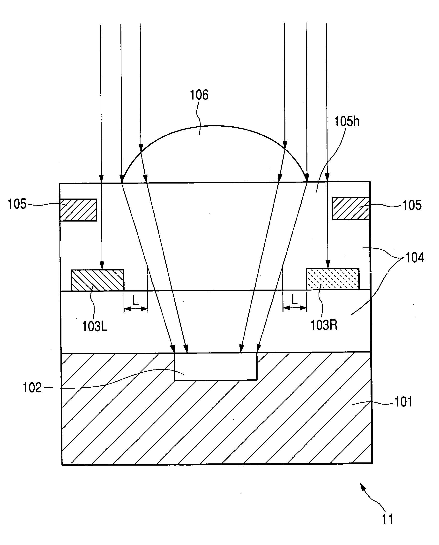
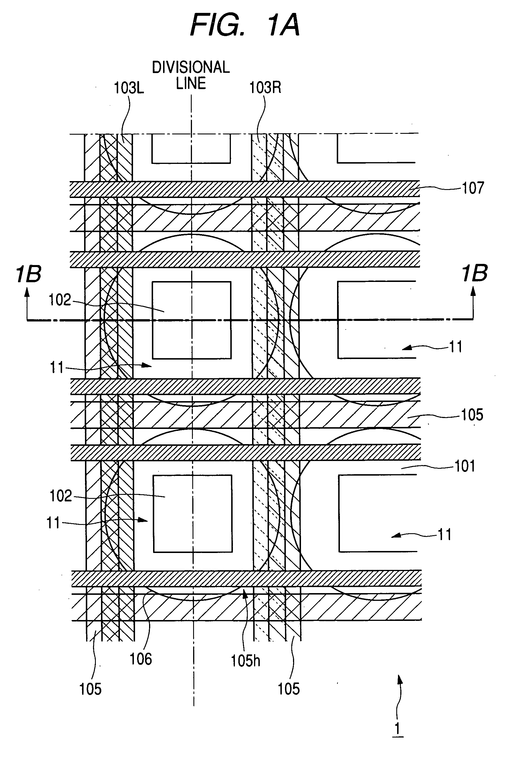
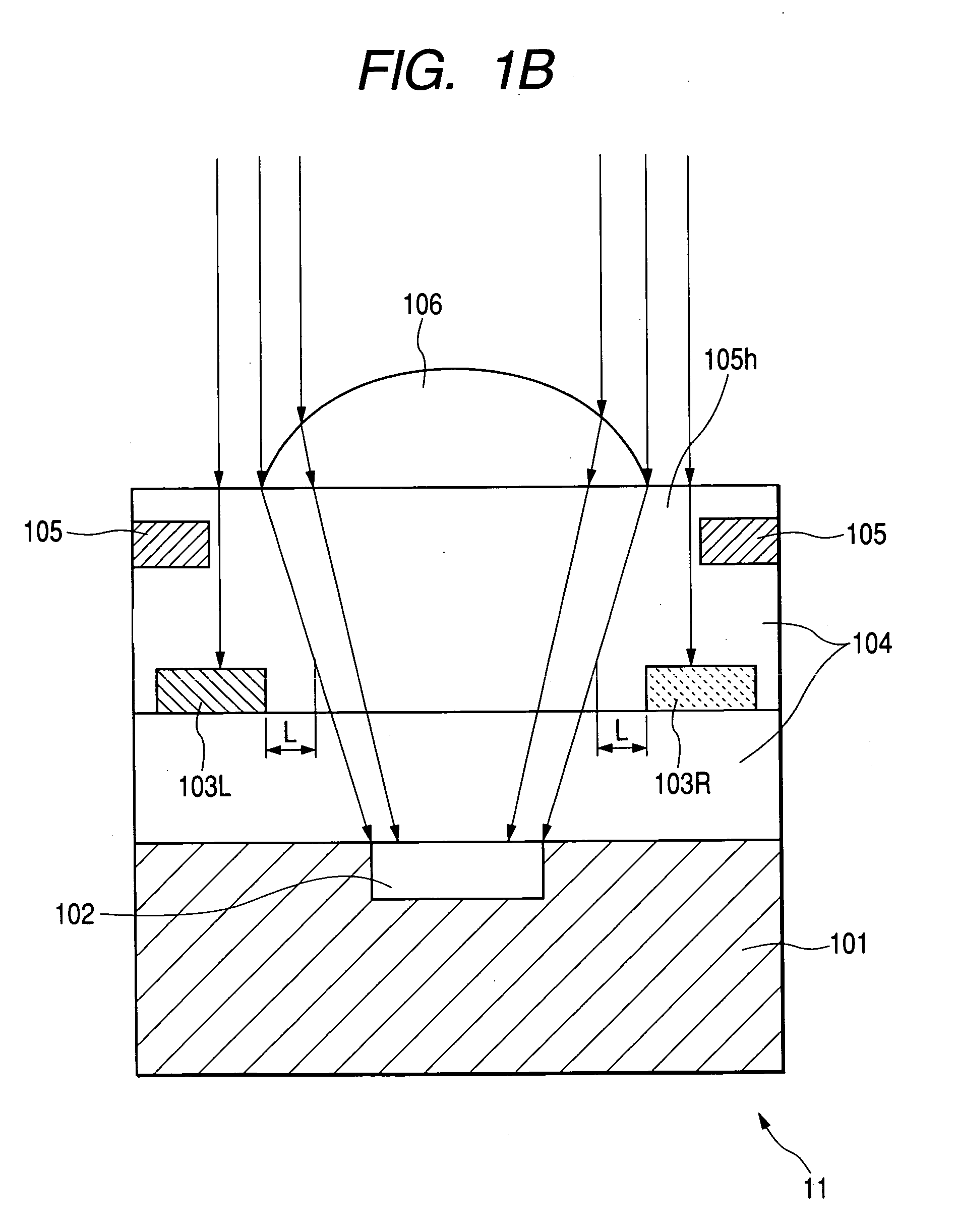
[0053]FIG. 1A is a top view showing wiring of an image pickup device according to the first embodiment, which is produced by a production method of the present invention. FIG. 1B is a sectional view showing an image pickup element of the image pickup device taken along a line 1B-1B in FIG. 1A.

[0054] As shown in FIGS. 1A and 1B, an image pickup device 1 has a plurality of image pickup elements 11 arranged in a matrix form at predetermined spaces on a substrate 101.

[0055] As shown in FIG. 1B, the image pickup element 11 has a light receiving area 102 having a photoelectric conversion element (not shown) formed thereon, an insulation layer 104 deposited on a substrate 101 in such a manner as to cover the light receiving area 102, and a microlens 106 placed on the surface of the insulation layer 104. The materials of components and methods for forming them are almost same as those of a well known image pickup element, and therefore detailed descriptions thereof are not presented. The ...

second embodiment

[0078] The opening 105h of the metal wiring 105 is formed with a sufficient clearance from the optical path for incident light as shown in FIG. 1B in the first embodiment, but the opening of metal wiring may be smaller so that the optical path for incident light is substantially regulated.

[0079] An image pickup element 12 shown in FIG. 3 has a smaller opening of metal wiring 105′ compared with the image pickup element 11 of the first embodiment shown in FIG. 1A, but is same as the image pickup element 11 for other configurations, and structural parts having same functions are given symbols identical to those of FIG. 1B and the descriptions thereof are not presented.

[0080] The metal wiring 105′ is designed so that the center of its opening is located on an optical axis of the microlens 106. It is designed so that incident light collected by the microlens 106 passes through the opening to the light receiving area 102. In this way, by reducing the opening of the metal wiring 105′, th...

third embodiment

[0082] An insulation layer may be composed of two or more layers having different refraction indexes. The image pickup element 13 shown in FIG. 4 has an insulation layer 104 and an insulation layer 204 having a refraction index smaller than that of the insulation layer 104. Other configurations are same as those of the image pickup element 12 of FIG. 3, and components having same functions are given symbols identical to those of FIG. 3 and the descriptions thereof are not presented.

[0083] In the image pickup element 13, the insulation layer 204 having a refraction index smaller than the insulation layer 104 is formed between the metal wiring 105′ and the patterns 103L and 103R. In this way, incident light collected by the microlens 106 passes through the insulation layer 104 and incidents into the insulation layer 204 and is then refracted toward the optical axis at the interface between the insulation layers 104 and 204. Then, when the incident light enters the insulation layer 10...


PUM


Abstract

The present invention inhibits variations in sensitivity of an image pickup element formed in a jointed area in the image pickup element produced using exposure in a joined fashion.
The image pickup element 11 has a light receiving area 102 formed on a substrate 101, an insulation layer 104 deposited on a light receiving area 102, and a microlens 106 formed on the insulation layer 104 and collecting incident light onto the light receiving area 102. A pattern 103L and a pattern 103R with an optical axis of the microlens 106 as a divisional line by exposure in a joined fashion in different exposure steps are arranged with an optical path for incident light collected by the microlens 106 held therebetween, and are provided so that a clearance from the optical path equals a distance L. The distance L is set to be larger than the alignment accuracy of an exposure device exposing the patterns 103L and 103R.

Description

BACKGROUND OF THE INVENTION [0001] 1. Field of the Invention [0002] The present invention relates to a solid image pickup device having a plurality of solid image pickup elements comprising photoelectric conversion elements, a method for producing the same, and an image pickup system comprising the solid state image pickup device. [0003] 2. Related Background Art [0004] A solid state image pickup device (hereinafter referred to simply as an image pickup device) having arranged one-dimensionally or two-dimensionally solid state image pickup elements (hereinafter referred to simply as image pickup elements) comprising light receiving areas having photoelectric conversion elements formed thereon is mounted as an area sensor on, for example, a digital camera, video camera, copier, facsimile or the like. Image pickup elements include, for example, CCD image pickup elements and amplification type image pickup elements. [0005] An example of a circuit configuration of an amplification type ...

Claims


Application Information

Patent Timeline
IPC IPC(8): H01L27/14H01L27/146H01L31/0232H04N5/225H04N5/335H04N5/369
CPCH01L27/14623H01L31/0232H01L27/14627H01L31/02327
Inventor OKITA, AKIRAHIYAMA, HIROKITAKADA, HIDEAKI
Owner CANON KK
Why Eureka
Try Eureka