Solid-state imaging device and electronic device

A solid-state imaging device and pixel technology, which is used in semiconductor/solid-state device manufacturing, radiation control devices, televisions, etc., can solve the problems of increased metal wiring wiring capacitance and reduced conversion efficiency, and achieves reduced parasitic capacitance, enhanced conversion efficiency, and enhanced The effect of pixel conversion efficiency

Active Publication Date: 2012-01-18
SONY SEMICON SOLUTIONS CORP
View PDF4 Cites 0 Cited by
  • Summary
  • Abstract
  • Description
  • Claims
  • Application Information

AI Technical Summary

Problems solved by technology

In the pixel sharing structure, the floating diffusion FD is often divided, and in addition to the parasitic capacitance of the diffusion region due to each divided floating diffusion FD, the wiring capacitance of the metal wiring connecting the divided floating diffusion FD increase, the conversion efficiency decreases compared to the case where the pixel sharing structure is not used

Method used


Image

  • Solid-state imaging device and electronic device
  • Solid-state imaging device and electronic device
  • Solid-state imaging device and electronic device

Examples


example

[0095] Some examples of the present invention will be described.

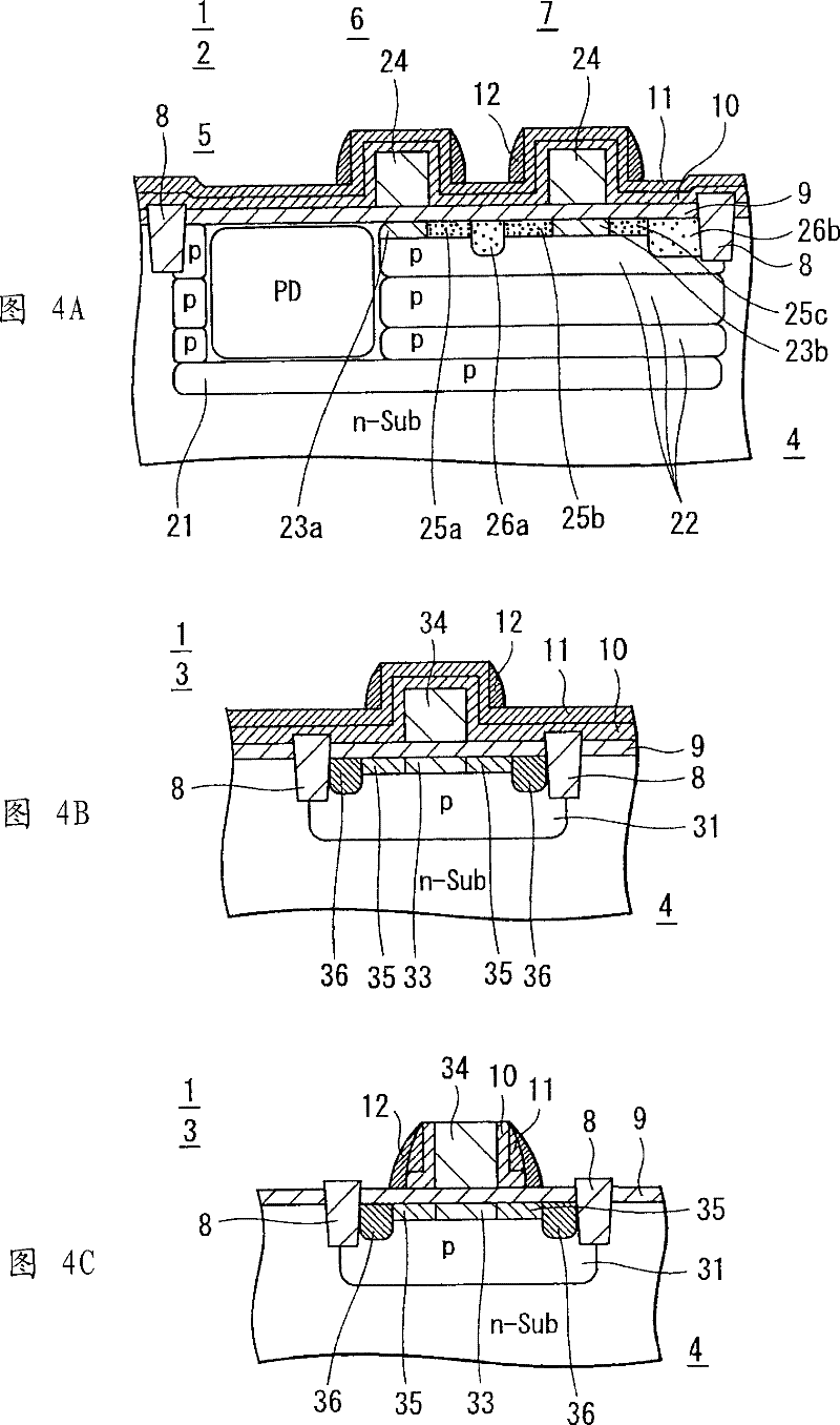
[0096] The first example of the invention will refer to Figures 21A to 21C to describe.

[0097] In the solid-state imaging device 1 in this example, the doping concentration in the FD, specifically, the doping concentration in the extended implant region 25a of the pixel 2 is lower than that in the impurity diffusion layer of the transistor of the peripheral circuit 3 . According to the impurity diffusion layer in the transistor of the peripheral circuit 3, usually the extended implantation region 25a has a surface impurity concentration of 1×10 20 / cm 3 or more to inject impurities. However, in the solid-state imaging device 1 of the present example, the impurity concentration of the extended implant region 25a is as low as one-tenth to one-hundredth of the surface impurity concentration.

[0098] Image quality may be prioritized in this configuration because contact resistance typically increases, but ...


PUM


Abstract

The present invention provides a solid-state imaging device which comprises the imaging areas arranged to a plurality of pixels of the two-dimension matrix and a peripheral circuit that detects the output signal from the pixels and the making method thereof, and also provides an electric device comprising the solid-state imaging device. The impurity concentration in transistor of each pixel is lower than that in the transistor of peripheral circuit. Besides, the impurity concentration of the semiconductor well region at the lower side of the floating diffusing part of the pixel is arranged tolower than that of semiconductor well region at the lower side of the transistor part at the back segment of the floating diffusing part.

Description

technical field [0001] The present invention relates to a solid-state imaging device, a manufacturing method thereof, and an electronic device including the solid-state imaging device. Background technique [0002] A CMOS (Complementary Metal Oxide Semiconductor) solid-state imaging device (CMOS image sensor) is a solid-state imaging device that has attracted attention especially in recent years. Such a CMOS solid-state imaging device includes an imaging area having a plurality of pixels arranged in a two-dimensional matrix, and peripheral circuits provided around the imaging area. In the imaging area, each pixel has: a floating diffusion layer (FD), which converts the charge from the photoelectric conversion part (photodiode: PD) into a voltage signal; a transfer transistor, which transfers the charge from the photodiode to the floating a diffusion section; a reset transistor that resets charges of the floating diffusion section; and an amplification transistor that output...

Claims


Application Information

Patent Timeline
Patent Type & Authority Patents(China)
IPC IPC(8): H01L27/146H01L21/822H04N5/335H04N5/369H04N5/374
Inventor 佐藤麻纪大木进
Owner SONY SEMICON SOLUTIONS CORP
Why Eureka
Try Eureka