
Fan out type wafer level package structure and method of the same

a package structure and fan-out technology, applied in the field of semiconductor package structure, can solve the problems of reducing the yield, reducing the yield, and the frame package technology is already not suitable for advanced semiconductor dies, so as to reduce the cost of the package structure and increase the yield of the package structure

Active Publication Date: 2005-06-09
WEN KUN YANG
View PDF7 Cites 62 Cited by
  • Summary
  • Abstract
  • Description
  • Claims
  • Application Information

AI Technical Summary

Benefits of technology

[0015] Still another objective of the present invention is to avoid problems of signal coupling and signal interface.
[0016] Another objective of the present invention is to lower the cost of the package structure.
[0017] Still another objective of the present invention is to raise the yield of the package structure.

Problems solved by technology

It causes the packaging for the semiconductor dies to become more difficult and decrease the yield.
The earlier lead frame package technology is already not suitable for the advanced semiconductor dies due to the density of the pins thereof is too high.
Therefore, number of the pads is limited and a too short pitch among pads results in a problem of signal coupling or signal interface.
Moreover, the size of die gradually become smaller and the packaged IC of the die does not have standard size by some package technologies (such as chip size package), but test equipment, package equipment, etc. for some fixed sizes die or packages can not be kept on using.

Method used


Image

  • Fan out type wafer level package structure and method of the same
  • Fan out type wafer level package structure and method of the same
  • Fan out type wafer level package structure and method of the same

Examples


Embodiment Construction

[0033] Some sample embodiments of the invention will now be described in greater detail. Nevertheless, it should be recognized that the present invention can be practiced in a wide range of other embodiments besides those explicitly described, and the scope of the present invention is expressly not limited expect as specified in the accompanying claims.

[0034] Then, the components of the different elements are not shown to scale. Some dimensions of the related components are exaggerated and meaningless portions are not drawn to provide a more clear description and comprehension of the present invention.

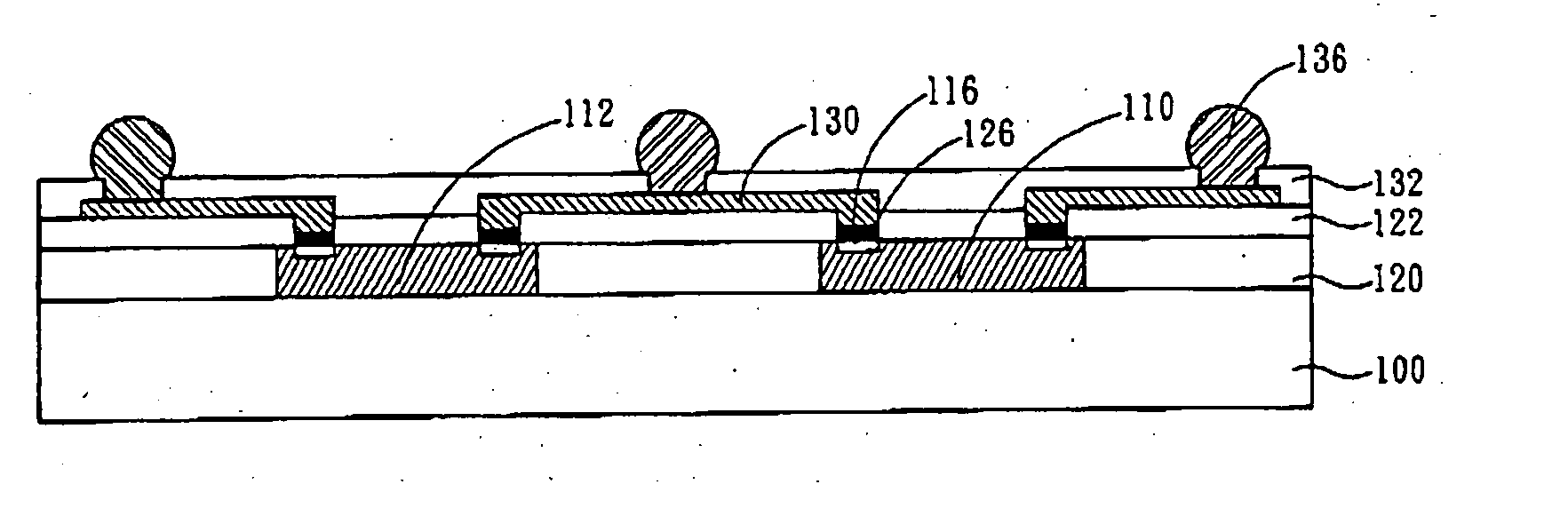
[0035] The essence of the present invention is to pick and place standard dies on a new base for obtaining an appropriate and wider distance between dies than the original distance of dies on a wafer. Therefore, the package structure has a larger size of balls array than the size of the die to avoid the problem of having too close ball pitch. Moreover, the die may be packaged with pa...


PUM


Abstract

To pick and place standard dies on a new base for obtaining an appropriate and wider distance between dies than the original distance of dies on a wafer. The package structure has a larger size of balls array than the size of the die by fan out type package. Moreover, the die may be packaged with passive components or other dies with a side by side structure or a stacking structure.

Description

BACKGROUND OF THE INVENTION [0001] 1. Field of the Invention [0002] This invention relates to a package for semiconductors, and more particularly to a fan out type wafer level package. [0003] 2. Description of the Prior Art [0004] The semiconductor technologies are developing very fast, and especially semiconductor dies have a tendency toward miniaturization. However, the requirements for the functions of the semiconductor dies have an opposite tendency to variety. Namely, the semiconductor dies must have more I / O pads into a smaller area, so the density of the pins is raised quickly. It causes the packaging for the semiconductor dies to become more difficult and decrease the yield. [0005] The main purpose of the package structure is to protect the dies from outside damages. Furthermore, the heat generated by the dies must be diffused efficiently through the package structure to ensure the operation the dies. [0006] The earlier lead frame package technology is already not suitable f...

Claims


Application Information

Patent Timeline
Patent Type & Authority Applications(United States)
IPC IPC(8): H01L21/44H01L21/48H01L21/50H01L21/58H01L21/60H01L23/12H01L23/00H01L23/14H01L23/31H01L23/48H01L23/485H01L23/52H01L23/522H01L23/538H01L23/552H01L25/065
CPCH01L21/561H01L2224/0401H01L23/5389H01L24/19H01L24/20H01L24/97H01L25/0655H01L25/0657H01L2224/04105H01L2224/20H01L2224/211H01L2224/97H01L2225/06524H01L2225/06541H01L2225/06551H01L2924/01013H01L2924/01015H01L2924/01027H01L2924/01029H01L2924/01033H01L2924/01074H01L2924/01075H01L2924/01077H01L2924/01078H01L2924/01079H01L2924/01082H01L2924/09701H01L2924/14H01L2924/15173H01L2924/15311H01L2924/19041H01L23/3128H01L2224/12105H01L2224/92244H01L2224/73267H01L2924/01005H01L2924/01006H01L2924/01019H01L2924/01068H01L2924/01076H01L2224/24137H01L2224/24195H01L2224/32225H01L2224/82H01L2924/15788H01L2924/00H01L23/48
Inventor YANG, WEN-KUNYANG, WEN-PINCHEN, SHIH-LI
Owner WEN KUN YANG
Features
  • Generate Ideas
  • Intellectual Property
  • Life Sciences
  • Materials
  • Tech Scout
  • Unparalleled Data Quality
  • Higher Quality Content
  • 60% Fewer Hallucinations
Learn More