

Selective polysilicon stud growth
- Summary
- Abstract
- Description
- Claims
- Application Information
AI Technical Summary
Benefits of technology
Problems solved by technology
Method used
Image

Examples
Embodiment Construction
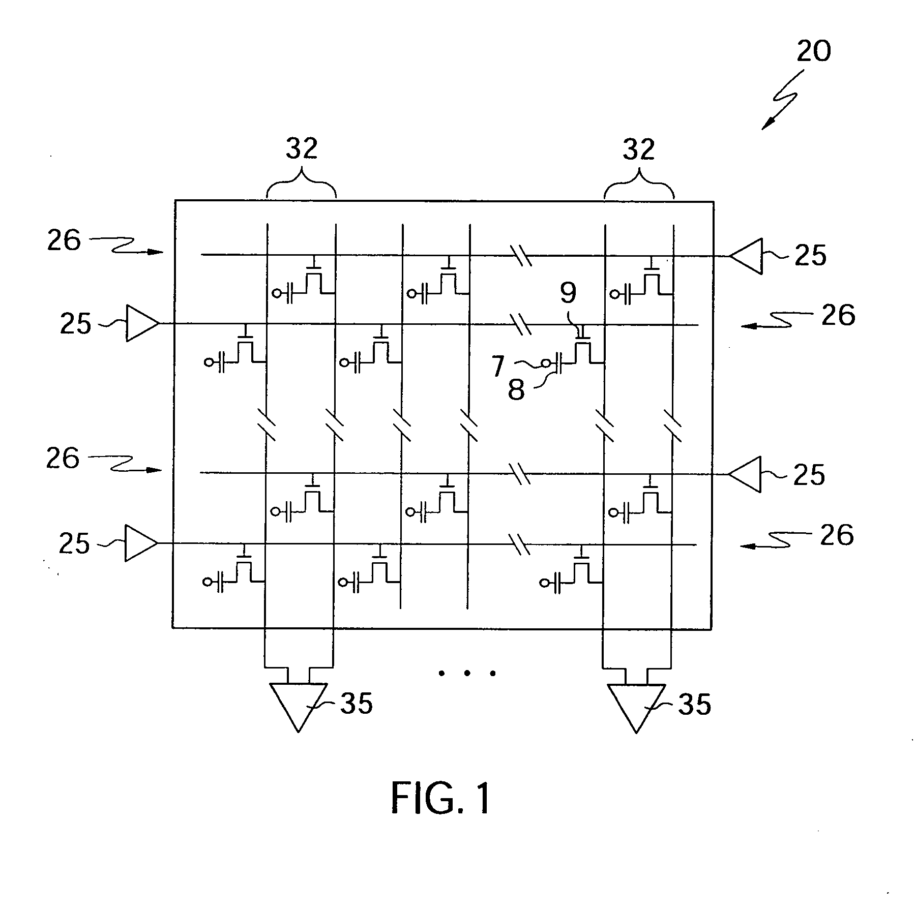
[0024]FIG. 1 is a schematic diagram of an exemplary memory array 20 in a memory device that includes word lines 26 running generally in parallel along one direction and bit line pairs 32 running generally in parallel along a perpendicular direction. A memory cell is represented schematically as a capacitor 8, and is connected by a transistor 9 to one of the bit line pairs 32. Each transistor 9 is activated by a word line 26 coupled to a word line driver 25. A row of memory cells 8 is selected upon activation of a word line 26. The state of each memory cell 8 in the row is transferred to a bit line 32 for sensing by sense amplifiers 35, each connected to a pair of bit lines 32. Respective cell plates 7 are illustrated schematically. Typically, as will be appreciated by those practicing the present invention and familiar with memory array structure, the bit lines 32 are twisted in the array 20.
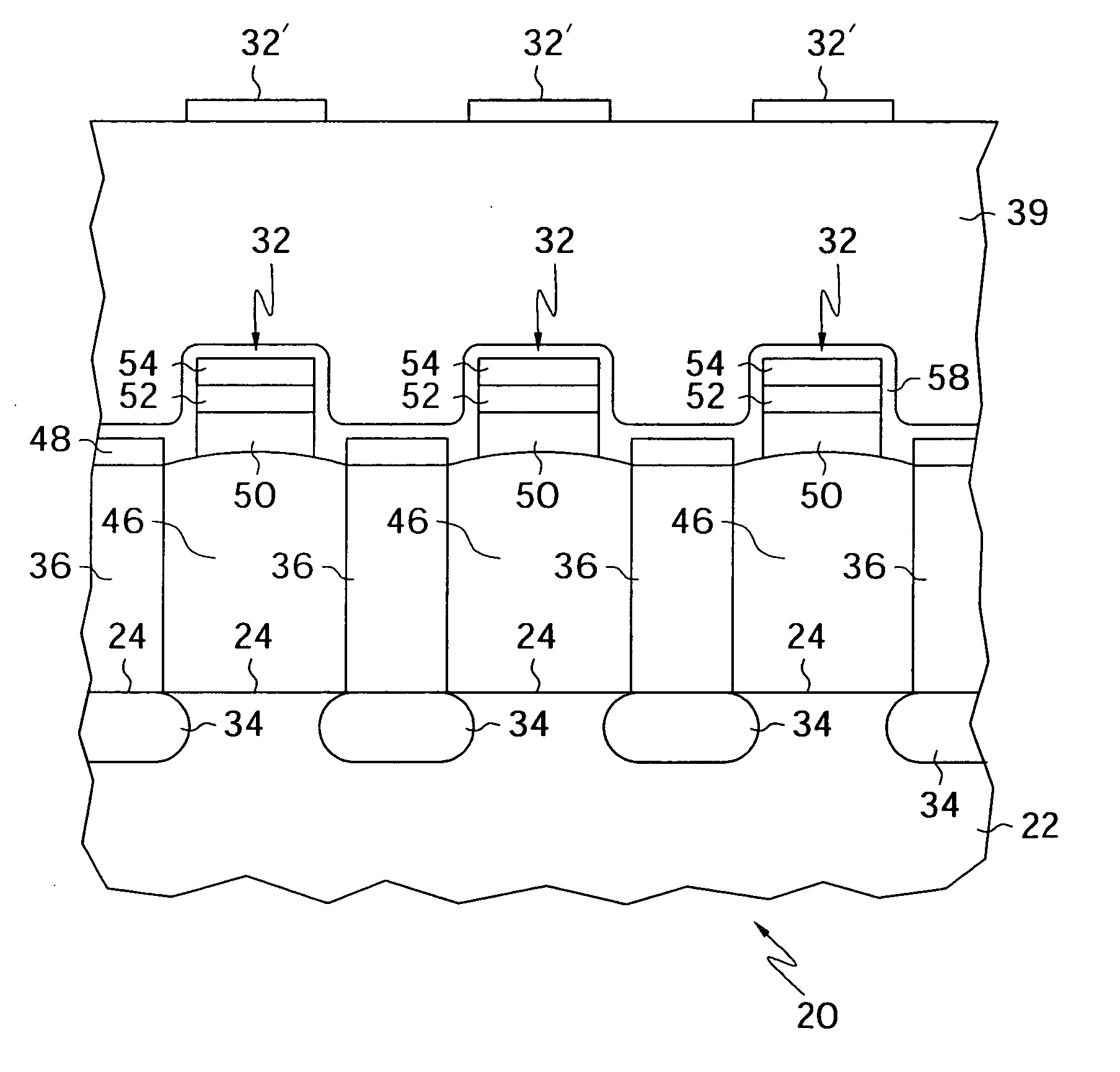
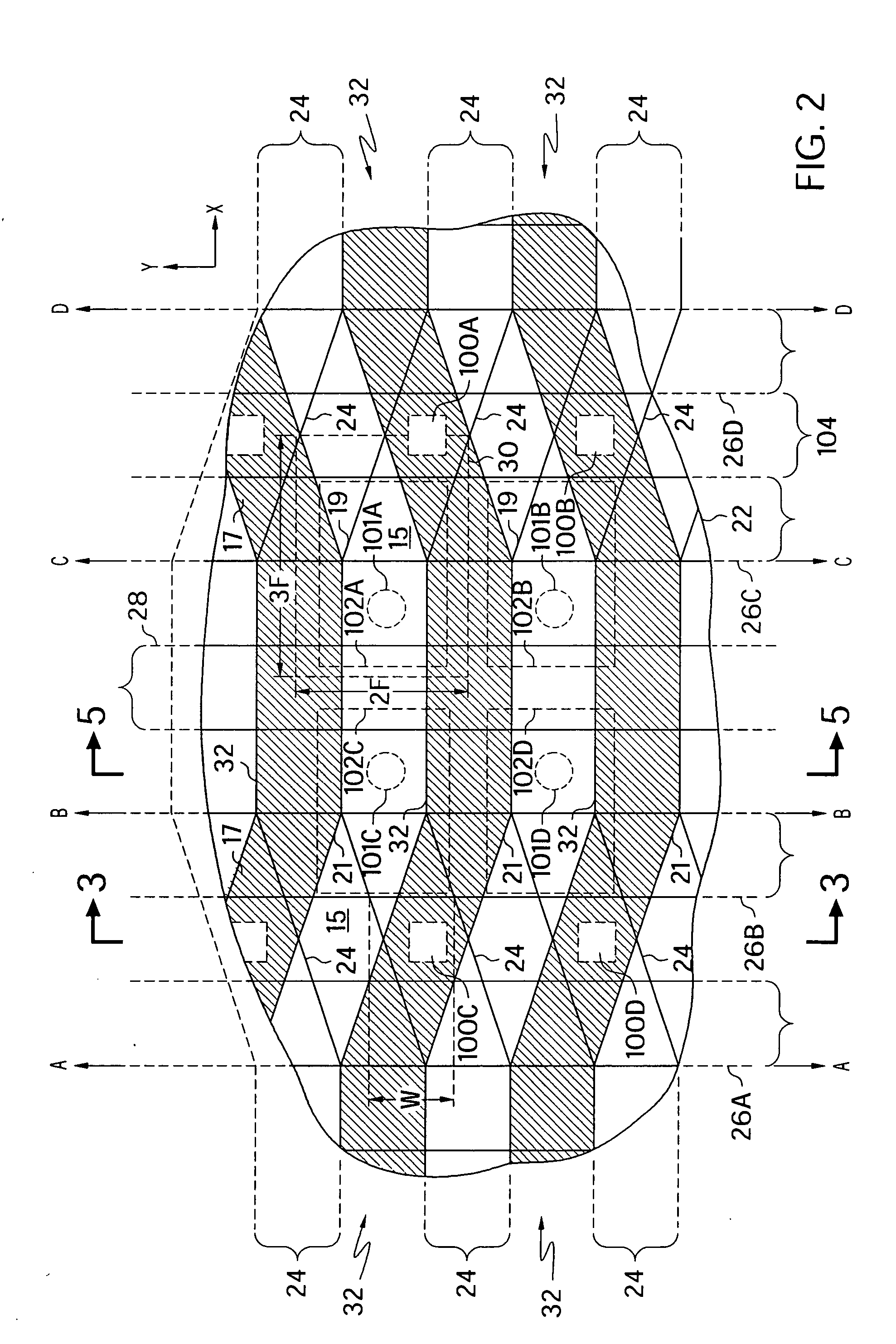
[0025]FIG. 2 shows the layout of a portion of the memory array of a semiconductor memory de...
PUM
| Property | Measurement | Unit |
|---|---|---|
| Electrical conductivity | aaaaa | aaaaa |
| Electrical conductor | aaaaa | aaaaa |
| Surface | aaaaa | aaaaa |
Abstract
Description
Claims
Application Information