Electromagnetic shield film, electromagnetic shield unit and display

a technology of electromagnetic shield and electromagnetic shield, applied in the field of electromagnetic shield unit and display, can solve the problems of increasing electromagnetic wave-related problems, increasing the number of electromagnetic shield films, so as to achieve the effect of easy thinning of the metal layer

Inactive Publication Date: 2004-04-22
HITACHI CHEM CO LTD
View PDF6 Cites 28 Cited by
  • Summary
  • Abstract
  • Description
  • Claims
  • Application Information

AI Technical Summary

Benefits of technology

0128] (1) First of all, the transparent base 2 is prepared. A metal layer is laminated on the transparent base 2 using the adhesive 3. Specifically, the metal foil is bonded onto the transparent base 2 by applying the adhesive 3 to either the metal foil or the transparent base 2 or to both of them. Then, the metal foil and transparent base 2 are dried. Any known bonding and drying processes are applicable. Further, the metal foil may be bonded by pressure application, a roll laminating process, or an autoclaving process, for example. The roll laminating process is most preferable in view of workability and economical efficiency
0129] The metal layer may be formed also by bonding the metal foil on an adhesive layer using the vacuum deposition process, sputtering process, ion plating process, chemical vapor deposition process, electroless or electric plating, or by using two or more of the foregoing processes. These processes are effective in easily thinning the metal layer. Further, the adhesive 3 may be dispensable when the foregoing processes are adopted.

Problems solved by technology

Electromagnetic waves radiated from electric and electronic devices have become one of serious social problems.
Such electromagnetic waves tend to reach adjacent devices as noise or erroneously operate them.
As more electric and electronic devices are used and computers are used to control such electric and electronic devices, electromagnetic wave-related problems increase and inevitably become more serious and unpredictable.
Further, it is pointed out that electromagnetic waves result in health hazard.
However, the foregoing measures tend to adversely affect the most important feature, i.e. visibility of images on the display.
In the foregoing case, it is very difficult to smoothly and uniformly bond the conductor and the earth portion on the transparent base.
Air bubbles are sometimes present between the transparent base and the conductor and between the transparent base and the earth portion, which causes non-uniform or insufficient bonding.
To overcome this problem, it is conceivable to use a very strong adhesive, which might put a limit on productivity or adversely affect mass productivity.
Further, if the electromagnetic wave shield filter is directly integrated to a display cabinet or to a display body, it is also very difficult to bond the transparent base and conductive members smoothly and reliably.
Air bubbles may be present between the transparent base and the conductive members, which will cause partial contact or bonding thereof.
This will reduce electromagnetic wave shielding performance and damage the display body.

Method used


Image

  • Electromagnetic shield film, electromagnetic shield unit and display
  • Electromagnetic shield film, electromagnetic shield unit and display
  • Electromagnetic shield film, electromagnetic shield unit and display

Examples


second example

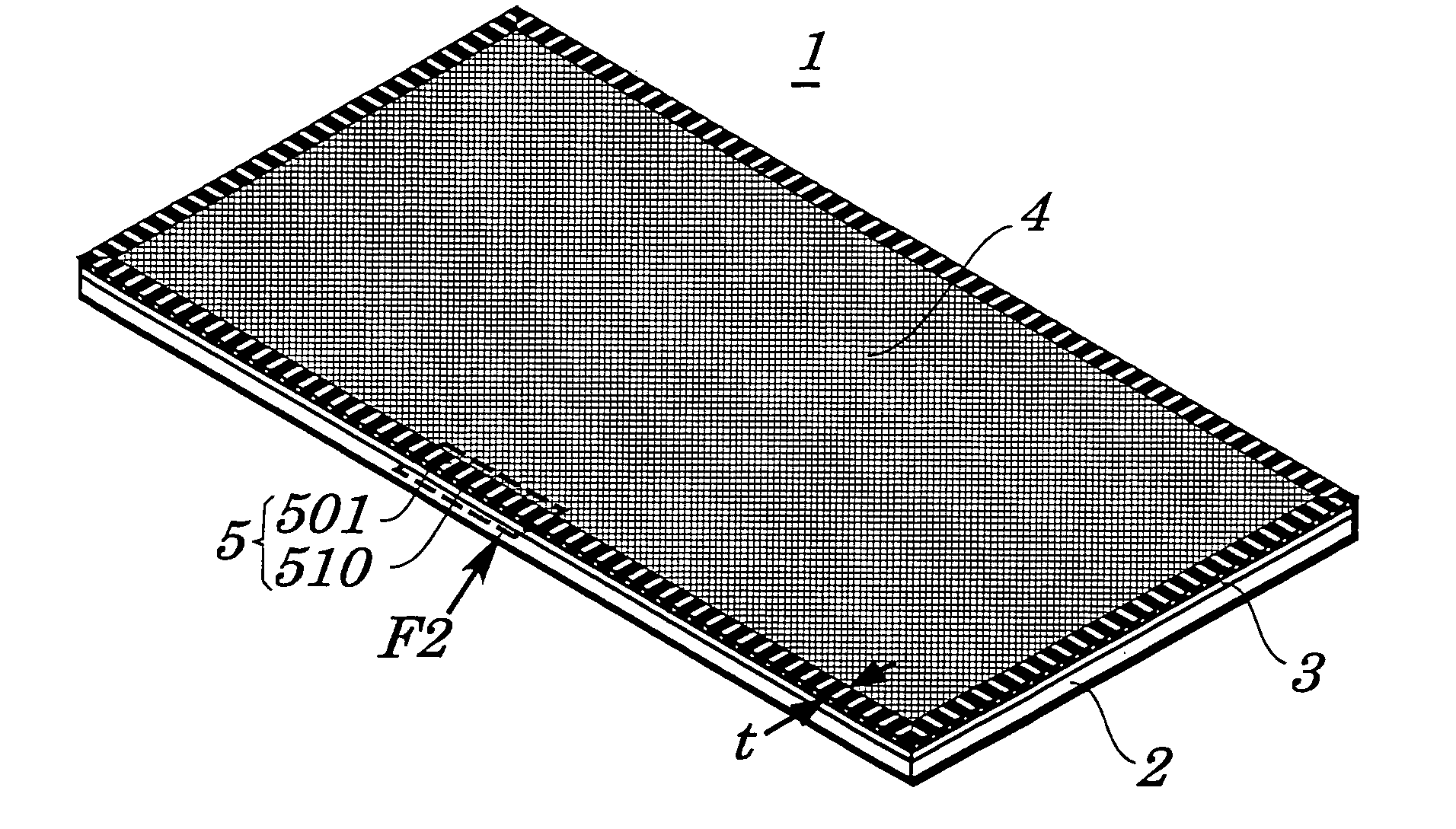
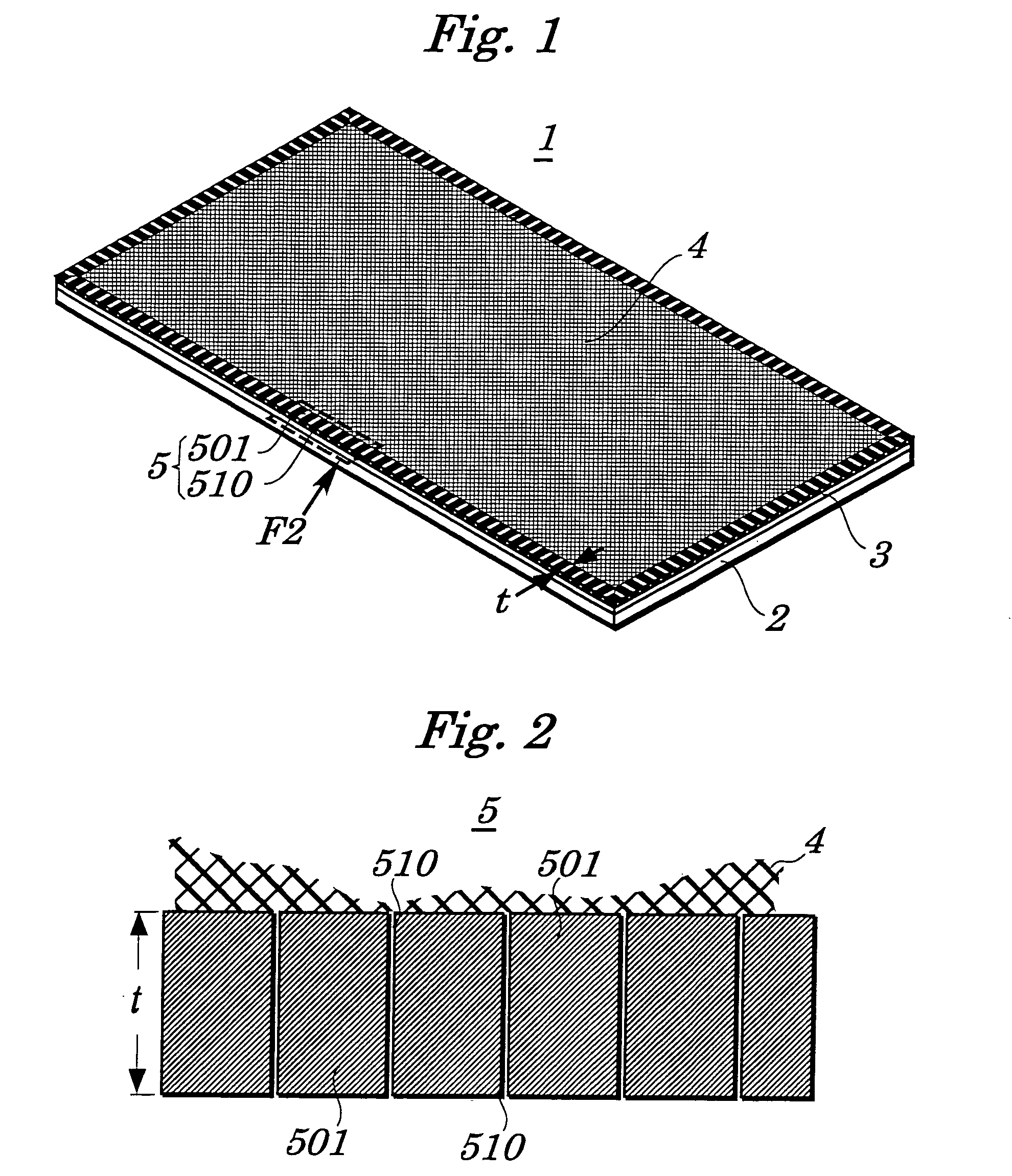
[0146] The forgoing conditions are applied in order to make conductor 4 with the mesh geometric pattern, the earth portion 5 having the conductive regions 501 with the rectangular geometric pattern (shown in FIG. 18) and the non-conductive regions 510 in the shape of a slit. The earth portion 5 of FIG. 18 is identical to the earth portion 5 having the first structure, shown in FIG. 2. In this example, the conductive region 501 has a length L2 of 100 mm while the slit width W2 is 5 mm.

[0147] As described in the first example, after the chemical etching, the surface of the adhesive 3 becomes opaque because the coarse surface of the copper foil has been transferred thereto. In order to obtain the transparent electromagnetic wave shield film 1 having the second structure, the surface of the copper foil on the conductive regions 501 and the adhesive PET film as the adhesive 3 are heated and pressed under the conditions of 120.degree. C. and 49.times.10.sup.4 Pa.

third example

[0148] The conditions mentioned in the first example are also applied in this example. The conductor 4 has the mesh geometric pattern while the earth portion 5 includes the comb-shaped conductive regions 501 and the slit-shaped non-conductive regions 510, as shown in FIG. 19. The earth portion 5 shown in FIG. 19 is identical to the earth portion 5 having the third structure shown in FIG. 10. The length L3 of the conductive region 501 is 100 mm, the slit width W3 is 5 mm, and the length t1 of the non-conductive region 510 is 2 mm.

[0149] After the chemical etching, the surface of the adhesive 3 also becomes opaque because the coarse surface of the copper foil has been transferred thereto. In order to obtain the transparent electromagnetic wave shield film 1 having the second structure, the surface of the copper foil on the conductive regions 501 and the adhesive PET film as the adhesive 3 are heated and pressed under the conditions of 120.degree. C. and 49.times.10.sup.4 Pa.


PUM


Abstract

An electromagnetic wave shield film (1) comprises a transparent base (2), a conductor (4) positioned on the transparent base (2) via an adhesive (3) and having a mesh geometric pattern, and an earth portion (5) arranged around the conductor (4) and including conductive regions (501) which absorb electromagnetic waves, and non-conductive regions (510) which prevent the earth portion (5) from being creased.

Description

[0001] The present invention relates to an electromagnetic wave shield film, an electromagnetic wave shield unit and a display, and more particularly relates not only to an electromagnetic wave shield film which shields electromagnetic waves generated via a front part of a plasma display including a plasma display panel (PDP), a cathode ray tube (CRT) display, a liquid crystal display (LC), an electro luminescence display (EL) or the like, but also to an electromagnetic wave shield unit including the electromagnetic wave shield film and a display including the electromagnetic wave shield unit.[0002] Recently, computerization has been remarkably promoted and improved. Displays are one of essential items for the computerization, and are being used for a variety of devices such as television sets (TV), word processors, personal computers, analyzers, game machines, and vehicle-mounted monitors. Further, such displays have been extensively enlarged.[0003] Electromagnetic waves radiated f...

Claims


Application Information

Patent Timeline
Patent Type & Authority Applications(United States)
IPC IPC(8): H05K9/00
CPCH05K9/0096H05K9/00
Inventor TAKAHASHI, HIROAKIIMAIZUMI, JUNICHINAKAMURA, HAJIMENOMURA, HIROSHI
Owner HITACHI CHEM CO LTD
Why Eureka
Try Eureka