High-density plasma multilayer gate oxide

a multi-layer, gate oxide technology, applied in the direction of semiconductor devices, electrical apparatus, transistors, etc., can solve the problems of voids or defects, poor electrical performance of oxide or sub-oxide thin-films, and thermal oxidation process that is not suitable for low-temperature devices, so as to improve bulk and interfacial quality, improve thermal budget, and reduce the effect of oxidation efficiency

Inactive Publication Date: 2006-03-23
SHARP KK
View PDF12 Cites 30 Cited by
  • Summary
  • Abstract
  • Description
  • Claims
  • Application Information

AI Technical Summary

Benefits of technology

[0018] The present invention describes a high-density plasma oxidation process to improve the bulk and interfacial quality of Si oxide thin-films deposited on planar, stepped, graded, or curved surfaces. High-density plasma generated oxide radicals promote the efficient oxidation of the oxide thin-films at significantly lower thermal budgets than the thermal or conventional plasma oxidation processes. In this manner, good oxide step-coverage is achieved simultaneously with good oxide quality and reliability.
[0020] The present invention plasma oxidation process further addresses the issue of step-coverage for V-TFT devices, which require high step-coverage oxide processes to obtain uniform deposition on the top and side faces, which are perpendicular to each other. The step-coverage of conventional PECVD processes depends on the nature of precursor, process temperatures, and the plasma processing conditions. In general, any conventional attempt to improve the step-coverage results in a degradation of the electrical performance. The present invention post-deposition high-density plasma oxidation process enhances the bulk and interfacial quality of the oxide thin-film, even though the film has been deposited at low temperatures to achieve high step-coverage on graded or abrupt transition surfaces.
[0022] In one aspect, the second Si oxide layer is deposited using a plasma-enhanced chemical vapor deposition (PECVD) process with tetraethylorthosilicate (TEOS) precursors. Advantageously, the second layer of SiOx can be additionally oxidized using the HDP source at a temperature of less than 400° C. One advantage to additionally oxidizing the second layer of SiOx, is that the concentration of oxide charges in the second SiOx layer can be decreased. Likewise, the first layer of SiOx can be grown using the HDP source at a temperature of less than 400° C.

Problems solved by technology

The oxidation state, and oxygen vacancies or defects are the major source of poor electrical performance of oxide or sub-oxide thin-films.
However as mentioned above, the thermal oxidation process is not suitable for low temperature devices due to high temperatures and large thermal budgets.
However, the conventional capacitively coupled plasma-based processes have high thermal budgets due to low plasma concentration and energy.
Structural damage can occur as a result of attempting to enhance the reaction kinetics by increasing the plasma power, which results in a corresponding increase in the sheath potential.
In general, any conventional attempt to improve the step-coverage results in a degradation of the electrical performance.

Method used


Image

  • High-density plasma multilayer gate oxide
  • High-density plasma multilayer gate oxide
  • High-density plasma multilayer gate oxide

Examples


Embodiment Construction

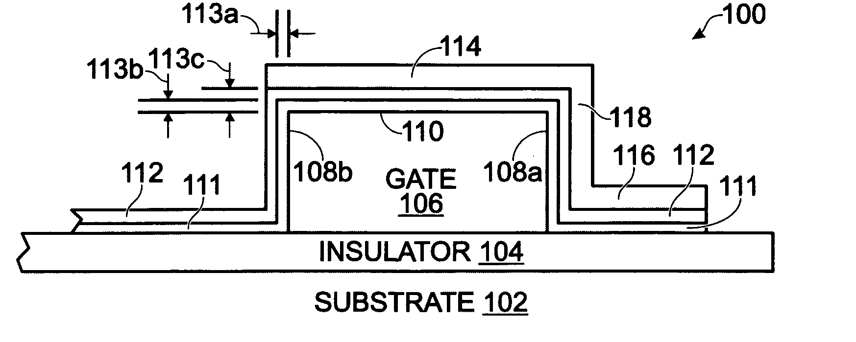
[0035]FIG. 1 is a partial cross-sectional view of a vertical thin-film transistor (V-TFT) device. The V-TFT 100 comprises a substrate 102 and a substrate insulation layer 104 overlying the substrate 102. Generally, the substrate 102 can be a material such as glass, Si, Si , Si , quartz, plastic, or temperature-sensitive material. A gate 106, having vertical sidewalls 108 and a top surface 110, overlies the substrate insulation layer 104. A first Silicon oxide (SiOx) layer 111 overlies the gate top surface 110 and sidewalls 108 having a step-coverage of greater than 65%, where x is less than, or equal to 2. Likewise, a second SiOx layer 112 overlies the first SiOx layer 111, and has a step-coverage of greater than 65%. Together, the first Si oxide layer 111 and the second Si oxide layer 112 can be considered as the gate insulator or a gate insulator stack.

[0036] Using the first Si oxide layer 111 as an example, step-coverage is defined as the ratio of a vertical aspect thickness 113...


PUM


Abstract

A thin-film transistor (TFT) with a multilayer gate insulator is provided, along with a method for forming the same. The method comprises: forming a channel, first source / drain (S / D) region, and a second S / D region in a Silicon (Si) active layer; using a high-density plasma (HDP) source, growing a first layer of Silicon oxide (SiOx) from the Si active layer, to a first thickness, where x is less than, or equal to 2; depositing a second layer of SiOx having a second thickness, greater than the first thickness, overlying the first layer of SiOx; using the HDP source, additionally oxidizing the second layer of SiOx, wherein the first and second SiOx layers form a gate insulator; and, forming a gate electrode adjacent the gate insulator. In one aspect, the second Si oxide layer is deposited using a plasma-enhanced chemical vapor deposition (PECVD) process with tetraethylorthosilicate (TEOS) precursors.

Description

RELATED APPLICATIONS [0001] This application is a continuation-in-part of a pending patent application entitled, HIGH-DENSITY PLASMA OXIDATION FOR ENHANCED GATE OXIDE PERFORMANCE, invented by Joshi et al., Ser. No. 11 / 139,726, filed May 26, 2005. [0002] This application is a continuation-in-part of a pending patent application entitled, HIGH-DENSITY PLASMA PROCESS FOR SILICON THIN-FILMS, invented by Pooran Joshi, Ser. No. 10 / 871,939, filed Jun. 17, 2004. [0003] This application is a continuation-in-part of a pending patent application entitled, METHODS FOR FABRICATING OXIDE THIN-FILMS, invented by Joshi et al., Ser. No. 10 / 801,374, filed Mar. 15, 2004. [0004] This application is a continuation-in-part of a pending patent application entitled, VERTICAL THIN-FILM TRANSISTOR, invented by Schuele et al., Ser. No. 10 / 831,424, filed Apr. 23, 2004. The above-mentioned applications are incorporated herein by reference.BACKGROUND OF THE INVENTION [0005] 1. Field of the Invention [0006] This ...

Claims


Application Information

Patent Timeline
Patent Type & Authority Applications(United States)
IPC IPC(8): H01L29/786H01L21/84
CPCH01L21/02164H01L21/02274H01L21/02304H01L21/0234H01L29/78642H01L21/31612H01L29/4908H01L29/6675H01L21/28008
Inventor JOSHI, POORAN CHANDRAVOUTSAS, APOSTOLOS T.
Owner SHARP KK
Why Eureka
Try Eureka