High-density plasma oxidation for enhanced gate oxide performance

a gate oxide and high-density plasma technology, applied in the field of gate oxide, can solve the problems of poor electrical performance of oxide or sub-oxide thin-films, thermal oxidation process is not suitable for low-temperature devices, and vacancies or defects, so as to improve bulk and interfacial quality, promote efficient oxidation of oxide thin-films, and reduce thermal budget

a gate oxide and high-density plasma technology, applied in the field of gate oxide, can solve the problems of poor electrical performance of oxide or sub-oxide thin-films, thermal oxidation process is not suitable for low-temperature devices, and vacancies or defects, so as to improve bulk and interfacial quality, promote efficient oxidation of oxide thin-films, and reduce thermal budget

US20050218406A1Inactive Publication Date: 2005-10-06SHARP KK

Image

  • High-density plasma oxidation for enhanced gate oxide performance
  • High-density plasma oxidation for enhanced gate oxide performance
  • High-density plasma oxidation for enhanced gate oxide performance

Examples


Embodiment Construction

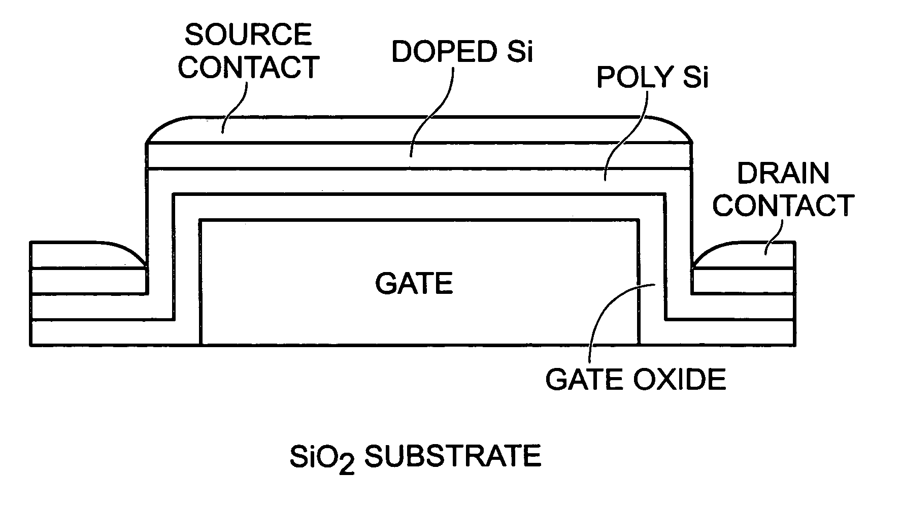
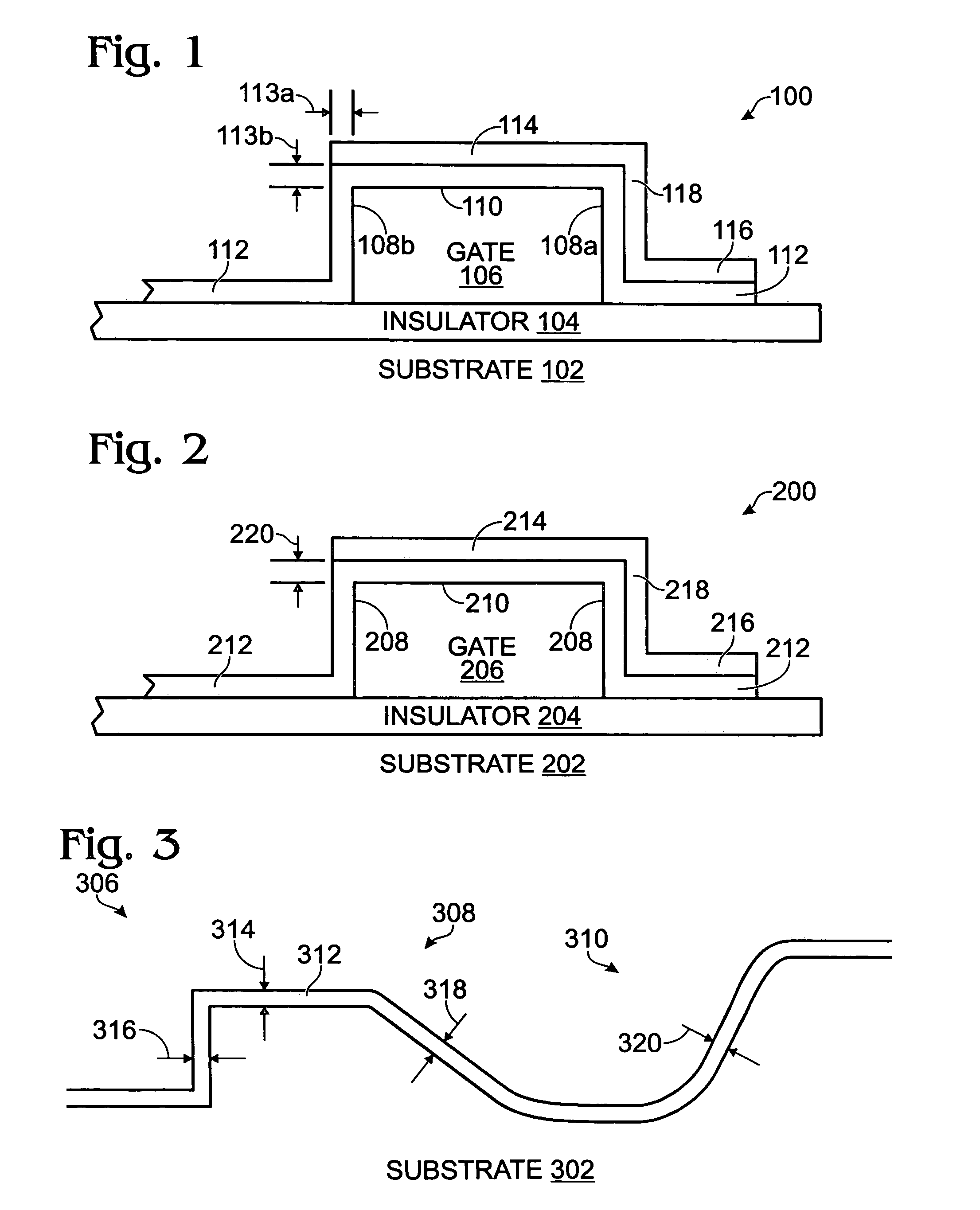
[0035]FIG. 1 is a partial cross-sectional view of a vertical thin-film transistor (V-TFT) device. The V-TFT 100 comprises a substrate 102 and a substrate insulation layer 104 overlying the substrate 102. Generally, the substrate 102 can be a material such as glass, silicon, or plastic. The substrate 102 can also be a temperature-sensitive transparent glass, quartz, or plastic material.

[0036] A gate 106, having vertical sidewalls 108 and a top surface 110, overlies the substrate insulation layer 104. A silicon oxide thin-film gate insulator 112 overlies the gate top surface 110 and sidewalls 108. The gate insulator 112 has a step-coverage of greater than 65%. Step-coverage is defined as the ratio of a vertical aspect thickness 113a, to a planar (horizontal) thickness 113b. As shown, the oxide thickness 113a over the sidewalls 108 is being compared to the oxide thickness 113b over the gate top surface 110. Poor step-coverage results in a relatively thin layer of oxide overlying corne...


PUM

PropertyMeasurementUnit
temperatureaaaaaaaaaa
thicknessaaaaaaaaaa
frequencyaaaaaaaaaa

Abstract

A method is provided for forming a low-temperature vertical gate insulator in a vertical thin-film transistor (V-TFT) fabrication process. The method comprises: forming a gate, having vertical sidewalls and a top surface, overlying a substrate insulation layer; depositing a silicon oxide thin-film gate insulator overlying the gate; plasma oxidizing the gate insulator at a temperature of less than 400° C., using a high-density plasma source; forming a first source / drain region overlying the gate top surface; forming a second source / drain region overlying the substrate insulation layer, adjacent a first gate sidewall; and, forming a channel region overlying the first gate sidewall, in the gate insulator interposed between the first and second source / drain regions. When the silicon oxide thin-film gate insulator is deposited overlying the gate a Si oxide layer, a low temperature deposition process can be used, so that a step-coverage of greater than 65% can be obtained.

Description

RELATED APPLICATIONS [0001] This application is a continuation-in-part of a pending patent application entitled, HIGH-DENSITY PLASMA PROCESS FOR SILICON THIN-FILMS, invented by Pooran Joshi, Ser. No. 10 / 871,939, filed Jun. 17, 2004. [0002] This application is a continuation-in-part of a pending patent application entitled, METHODS FOR FABRICATING OXIDE THIN-FILMS, invented by Joshi et al., Ser. No. 10 / 801,374, filed Mar. 15, 2004. [0003] This application is a continuation-in-part of a pending patent application entitled, VERTICAL THIN-FILM TRANSISTOR, invented by Schuele et al., Ser. No. 10 / 831,424, filed Apr. 23, 2004. These applications, and their parent applications, are incorporated herein by reference.BACKGROUND OF THE INVENTION [0004] 1. Field of the Invention [0005] This invention generally relates to the fabrication of integrated circuit (IC) devices, and more particularly, to a gate oxide and a method for forming the same using high-density plasma oxidation. [0006] 2. Descr...

Claims


Application Information

Patent Timeline
06 Oct 2005
Publication
US20050218406A1
IPC
H01L21/336; H01L21/84; H01L29/786
CPC
C23C16/24; C23C16/45523; C23C16/509; H01L29/78642; H01L21/31612; H01L29/66666; H01L29/6675; H01L21/049
Inventors
JOSHI, POORAN CHANDRA; VOUTSAS, APOSTOLOS T.