Dielectric ceramic composition and method of production and electronic device of the same

a technology of dielectric ceramics and electronic devices, applied in ceramics, fixed capacitors, electrical equipment, etc., can solve the problems of low frequency dielectric characteristic after firing deterioration, change of capacity, dielectric loss, etc., to improve the accelerated lifetime of insulation resistance, improve the low frequency dielectric characteristic, and increase reliability

Active Publication Date: 2005-06-16
TDK CORPARATION
View PDF4 Cites 70 Cited by
  • Summary
  • Abstract
  • Description
  • Claims
  • Application Information

AI Technical Summary

Benefits of technology

[0015] An object of the present invention is to provide a method for producing a reduction resistant dielectric ceramic composition having a superior low frequency dielectric characteristic and improved more in accelerated lifetime of the insulation resistance, a dielectric ceramic composition obtained by this method, and an electronic device such as a chip capacitor including the dielectric ceramic composition and raised more in reliability.
[0037] Preferably, the method has the step of firing the obtained dielectric ceramic composition at 1000 to 1400° C. The dielectric particles forming the dielectric ceramic composition obtained by the present invention have a mean crystal grain size of not more than 1 μm. The mean crystal grain size is calculated for example by the cord method. The inventors discovered that by controlling the mean crystal grain size of the dielectric particles forming the obtained dielectric ceramic composition, it is possible to improve the accelerated lifetime of the insulation resistance and as a result possible to improve the reliability of multilayer ceramic capacitors and other electronic devices produced using these dielectric ceramic composition.
[0044] The dielectric particles forming the dielectric ceramic composition obtained by this method are finely controlled to mean crystal grain sizes of not more than 1 μm. The inventors believe that making the mean crystal grain size of the dielectric particles finer in this way contributes to improvement of the lifetime. As a result, the reliability of the obtained electronic device is greatly improved.
[0045] That is, according to the present invention, it is possible to provide a method for producing a reduction resistant dielectric ceramic composition having a superior low frequency dielectric characteristic (for example, a dielectric loss of not more than 0.01% at 160° C. and 100 Hz) and further improved in accelerated lifetime of insulation resistance and a dielectric ceramic composition obtained by this method.
[0046] Further, the chip capacitor or other electronic device according to the present invention has dielectric layers formed by a dielectric ceramic composition produced by the method of the present invention, so has a superior capacity-temperature characteristic, is improved in accelerated lifetime of insulation resistance (high temperature load lifetime) while suppressing the low frequency dielectric dispersion, and as a result is greatly improved in reliability of the electronic device.

Problems solved by technology

However, in each of these dielectric ceramic compositions, the low frequency dielectric characteristic after firing deteriorated (change in capacity, dielectric loss) or the accelerated lifetime of the insulation resistance after firing became shorter.
Therefore, when using a dielectric ceramic composition to produce a multilayer ceramic capacitor having nickel or other base metal internal electrodes, the reliability of the multilayer ceramic capacitor obtained tended to fall.
However, even with the dielectric ceramic compositions described in Japanese Patent Publication (A) No. 2002-80278, Japanese Patent No. 2997236, and WO02 / 00568, a sufficient accelerated lifetime of insulation resistance is sometimes still not obtained.
As a result, when using a dielectric ceramic composition to produce a multilayer ceramic capacitor having nickel or other base metal internal electrodes, it is not possible to improve the reliability of a multilayer ceramic capacitor.
Even a person skilled in the art would find it difficult to determine which method is suitable for systems of different compositions without actual confirming experiments.

Method used


Image

  • Dielectric ceramic composition and method of production and electronic device of the same
  • Dielectric ceramic composition and method of production and electronic device of the same
  • Dielectric ceramic composition and method of production and electronic device of the same

Examples


example 1

[0104] In this example, a multilayer ceramic capacitor was produced by the following procedure.

[0105] Preparation of Pastes

[0106] First, the starting materials having mean particle sizes of 0.1 to 1 μm for producing the main component material (SrCO3, CaCO3, TiO2, ZrO2) and the first to fourth subcomponent materials were prepared. In this embodiment, a carbonate (third subcomponent MnCO3) was used for the material of the MnO, and oxides (first subcomponent V2O5, second subcomponent Al2O3, fourth subcomponent (Ba0.6Ca0.4)SiO3 (in the table, described as BCG)) were used for the other materials. Note that (Ba0.6Ca0.4)SiO3 were obtained by wet mixing BaCO3, CaCO3, and SiO2 by a ball mill for 16 hours, dried, then fired at 1000 to 1300° C. in the air and further wet pulverized by a ball mill for 100 hours.

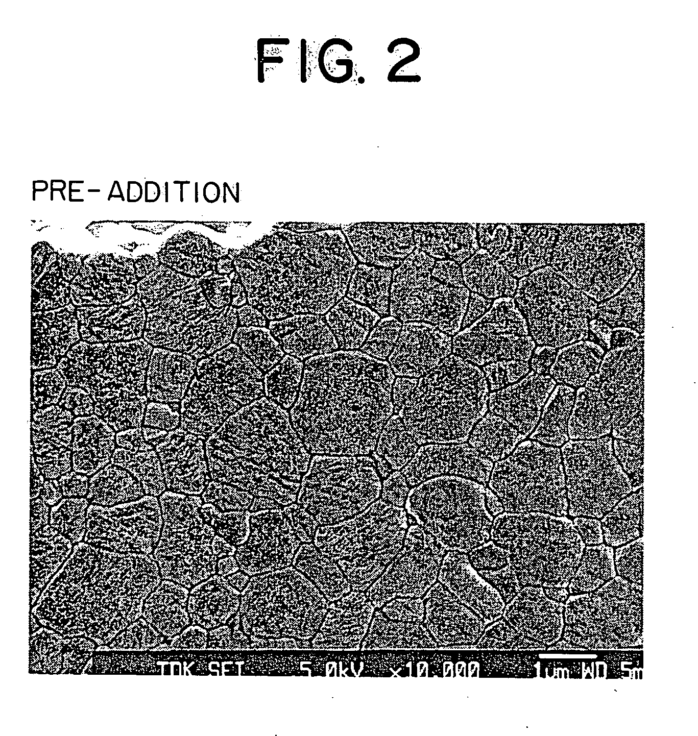
[0107] Next, a dielectric ceramic composition materials (powders) of the final compositions were obtained by pre-adding and post-adding the first to fourth subcomponent materials.

[0...

example 2

[0128] Except for changing the pre-addition and post-addition as shown in Table 2, the same procedure was followed as in Example 1 to prepare capacitor samples which were similarly evaluated for their characteristics. As a result, with each sample, tan δ was not more than 0.01%, the specific dielectric constant ε was at least 45, and the specific resistance ρ was at least 1×10¹² Ω·cm. Regarding the temperature characteristic of the static capacitance as well, the rate of change of the static capacitance with respect to the temperature satisfied −3000 to 0 ppm / ° C. The mean crystal grain size and the high temperature load lifetime are shown in Table 2. Note that the “pre-addition components” spoken of in this example means the subcomponent materials added to the starting materials for producing the main component material when producing the calcined material including the main component material. The “post-addition components” mean the subcomponent materials added to the calcined mat...

example 3

[0130] Except for changing the amounts of addition of the first to fourth subcomponents of the post-addition components as shown in. Table 3, the same procedure was followed as in Example 1 to prepare capacitor samples which were similarly evaluated for their characteristics. As a result, with each sample, tan δ was not more than 0.01%, the specific dielectric constant ε was at least 45, and the specific resistance ρ was at least 1×10¹² Ω·cm. Regarding the temperature characteristic of the static capacitance as well, the mean crystal grain size and the high temperature load lifetime are shown in Table 3. Note that the “post-addition component” spoken of in this example means subcomponent materials added to calcined material including the main component material.

TABLE 3Amount of addition of post-addition component1st subcomp.2nd subcomp.V2O3Al2O33rd subcomp.4th subcomp.CharacteristicsconversionconversionM conversionBCG conversionMean crystalHigh temp. loadSample(mol %)(mol %)(mol %...


PUM

PropertyMeasurementUnit
mean crystal grain sizeaaaaaaaaaa
grain sizeaaaaaaaaaa
grain sizesaaaaaaaaaa

Abstract

A method of production of a reduction resistant dielectric ceramic composition having a superior low frequency dielectric characteristic and further improved in accelerated lifetime of insulation resistance, specifically a method of production of a dielectric ceramic composition containing a main component including a dielectric oxide of a specific composition, a first subcomponent including a V oxide, a second subcomponent containing an Al oxide, a third subcomponent containing an Mn oxide, and a fourth subcomponent containing a specific sintering aid in a specific ratio, including a step of mixing at least part of the materials of the subcomponents excluding one or both of at least the material of the third subcomponent and material of the fourth subcomponent with the starting materials prepared for obtaining the material of the main component to prepare the pre-reaction material, a step of causing the prepared pre-reaction material to react to obtain a reacted material, and a step of mixing the materials of the subcomponents excluded when preparing the pre-reaction material with the obtained reacted material to obtain a dielectric ceramic composition.

Description

BACKGROUND OF THE INVENTION [0001] 1. Field of the Invention [0002] The present invention relates to a dielectric composition able to be used for example for dielectric layers of a multilayer ceramic capacitor and a method of production of the same and to an electronic device using this dielectric ceramic composition for dielectric layers. [0003] 2. Description of the Related Art [0004] In recent years, as dielectric ceramic compositions for forming multilayer ceramic capacitors etc., an example of an electronic device, various proposals have been made for the use of inexpensive base metals (for example, nickel, copper, etc.) for the materials for the internal electrodes (see Japanese Patent Publication (A) No. 11-224827, Japanese Patent Publication (A) No. 60-131708, Japanese Patent Publication (B) No. 57-37081, and Japanese Patent Publication (A) No. 63-126117). [0005] However, in each of these dielectric ceramic compositions, the low frequency dielectric characteristic after firi...

Claims


Application Information

Patent Timeline
Patent Type & Authority Applications(United States)
IPC IPC(8): C04B35/49C04B35/46C04B35/465C04B35/47C04B35/48H01B3/12H01G4/06H01G4/12H01G4/30
CPCB32B2311/22H01G4/30C04B35/47C04B35/49C04B35/62685C04B35/64C04B2235/3203C04B2235/3206C04B2235/3208C04B2235/3213C04B2235/3215C04B2235/3217C04B2235/3224C04B2235/3232C04B2235/3239C04B2235/3241C04B2235/3244C04B2235/3251C04B2235/3256C04B2235/3258C04B2235/3262C04B2235/3409C04B2235/3418C04B2235/3436C04B2235/3445C04B2235/3454C04B2235/5445C04B2235/6582C04B2235/6584C04B2235/662C04B2235/785C04B2235/786C04B2235/96C04B2237/346C04B2237/348C04B2237/405H01G4/1218C04B35/465C04B35/46C04B35/48H01B3/12
Inventor WATANABE, YASUOENDOH, KENTATAKAHARA, WATARU
Owner TDK CORPARATION
Why Eureka
Try Eureka