Semiconductor device and design-aiding program

a technology of semiconductor devices and semiconductors, applied in the field of vertical-type semiconductor devices, can solve problems such as the increase in on-resistance in consequence, and achieve the effects of reducing variation ratio, small variation ratio, and easy fabrication

Inactive Publication Date: 2005-06-23
DENSO CORP
View PDF22 Cites 31 Cited by
  • Summary
  • Abstract
  • Description
  • Claims
  • Application Information

AI Technical Summary

Benefits of technology

[0031] In accordance with the method for fabricating the new semiconductor device, when the first design-aiding program is used in a combination of the repetitive-pattern layer and the group of trench gate electrodes, a movement direction most reducing a variation ratio of a computed size of the overlap area is a direction parallel to the cutout face of the semiconductor substrate. When the second design-aiding program is used, on the other hand, a movement direction parallel to the cutout face of the semiconductor substrate is a direction most increasing a minimum value of a computed size of the overlap area. In general, in a process to create the group of trench gate electrodes on a semiconductor substrate, the position of the group is most likely shifted in a direction parallel to the cutout face of the semiconductor substrate. Thus, when the repetitive-pattern layer is created on the semiconductor substrate by execution of the first design-aiding program in the positional relationship cited above, a semiconductor device having a small variation ratio is easy to fabricate even if the position of the group of trench gate electrodes is shifted. When the repetitive-pattern layer is created on the semiconductor substrate by execution of the second design-aiding program, on the other hand, a channel resistance is at least reduced to a range of values not exceeding a predetermined upper limit even if the position of a trench gate electrode is shifted.

Problems solved by technology

In the conventional semiconductor device, there is a tradeoff that, when a characteristic exhibiting a high withstand voltage is implemented, the on-resistance increases in consequence.

Method used


Image

  • Semiconductor device and design-aiding program
  • Semiconductor device and design-aiding program
  • Semiconductor device and design-aiding program

Examples


first embodiment

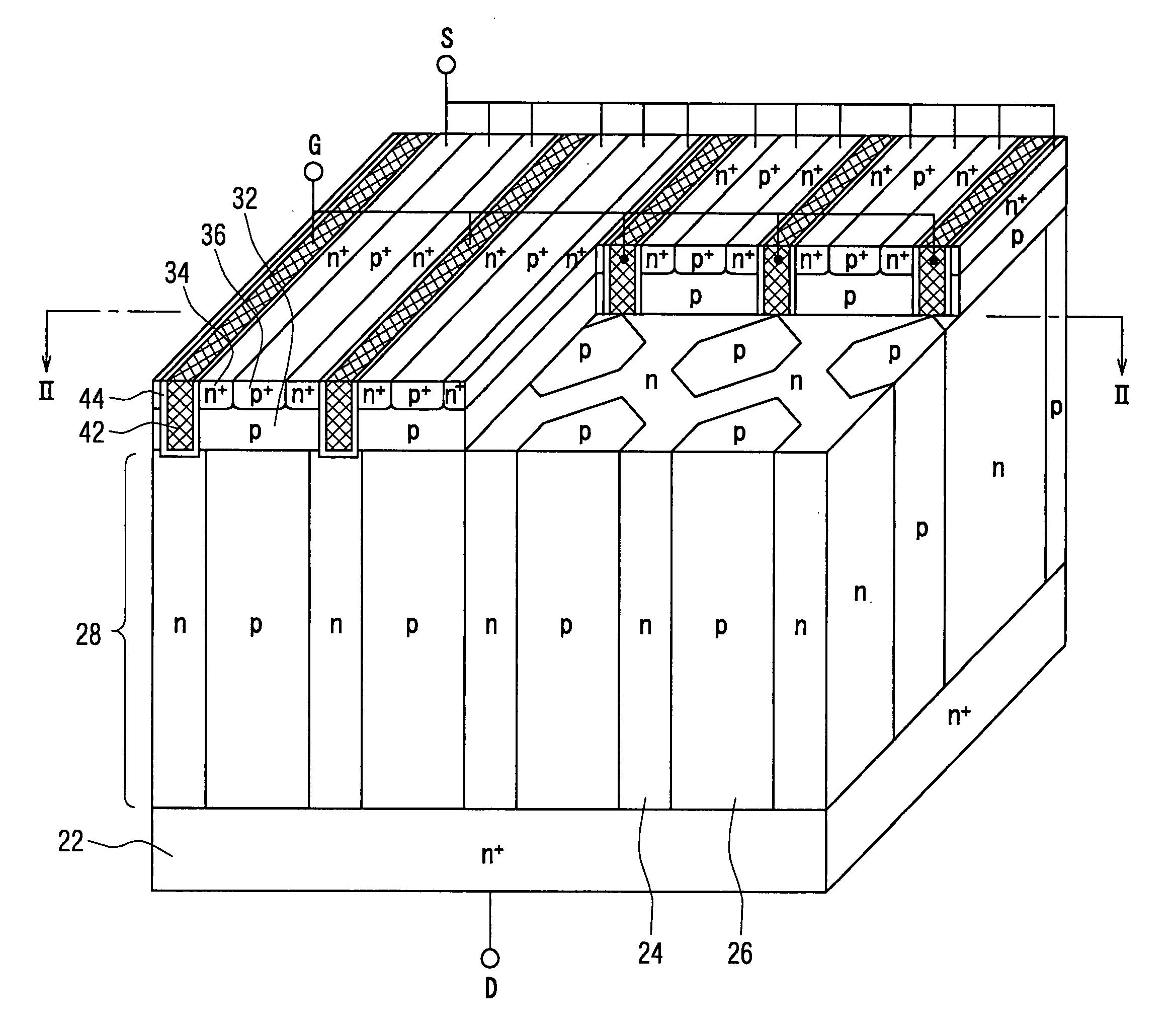
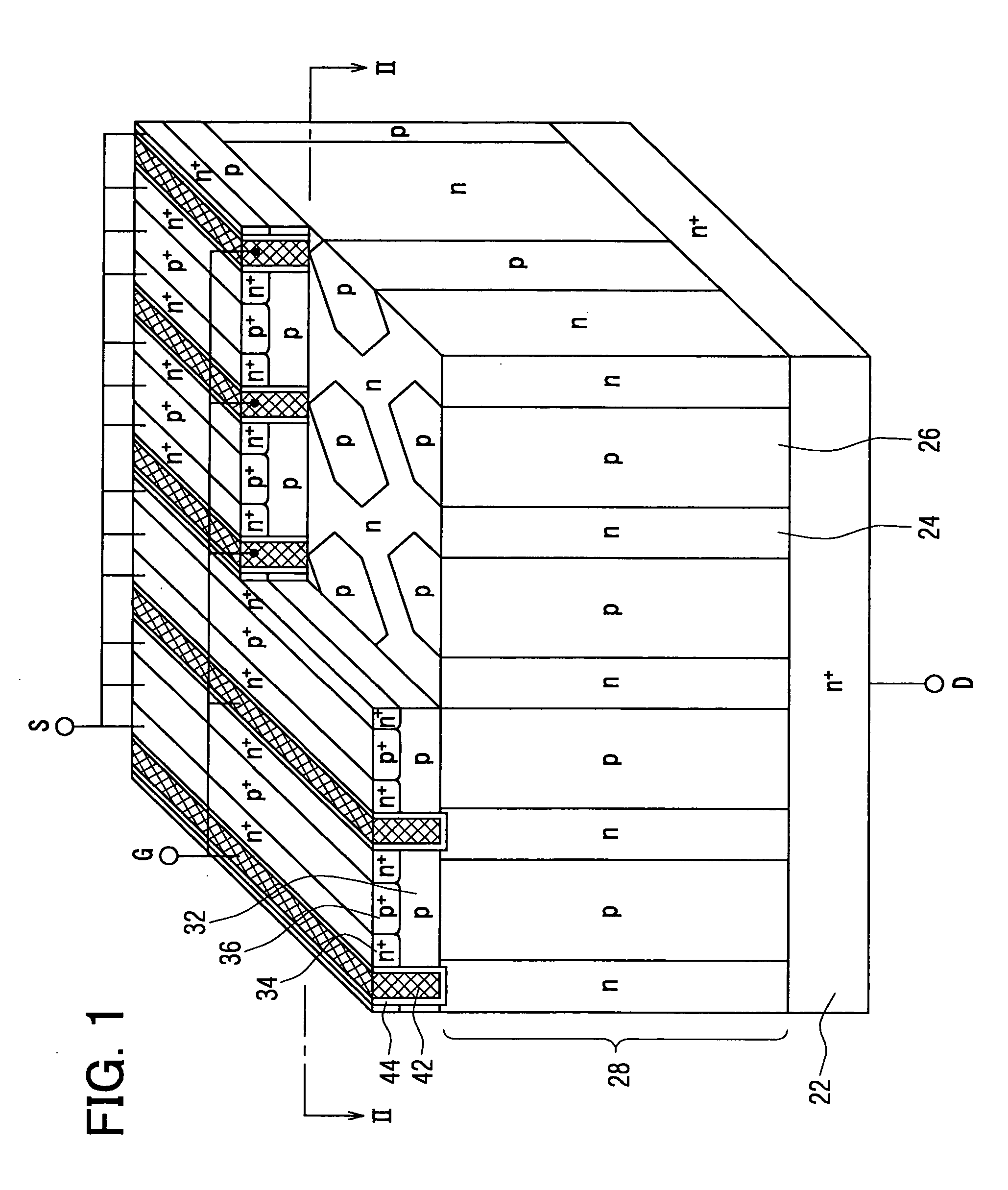
[0049]FIG. 1 is a diagram showing a perspective view of elements composing a semiconductor device including a repetitive-pattern structure of p-type columns 26 and n-type columns 24 on a withstand-voltage layer 28. The semiconductor device has a group of trench gate electrodes 42 each reaching a withstand-voltage layer 28 by penetrating a body layer 32 in contact with the withstand-voltage layer 28. The trench gate electrodes 42 are each created by extending the trench gate electrodes 42 straightly over a long distance on a face parallel to the principal face of the semiconductor device and are arranged repetitively in a direction perpendicular to the longitudinal direction of the group of trench gate electrodes 42 to form parallel stripes. A portion of the body layer 32 is cut out to expose an on-face pattern of the repetitive-pattern structure.

[0050] The semiconductor device shown in FIG. 1 is explained in more detail as follows. The repetitive-pattern structure of the semiconduc...

second embodiment

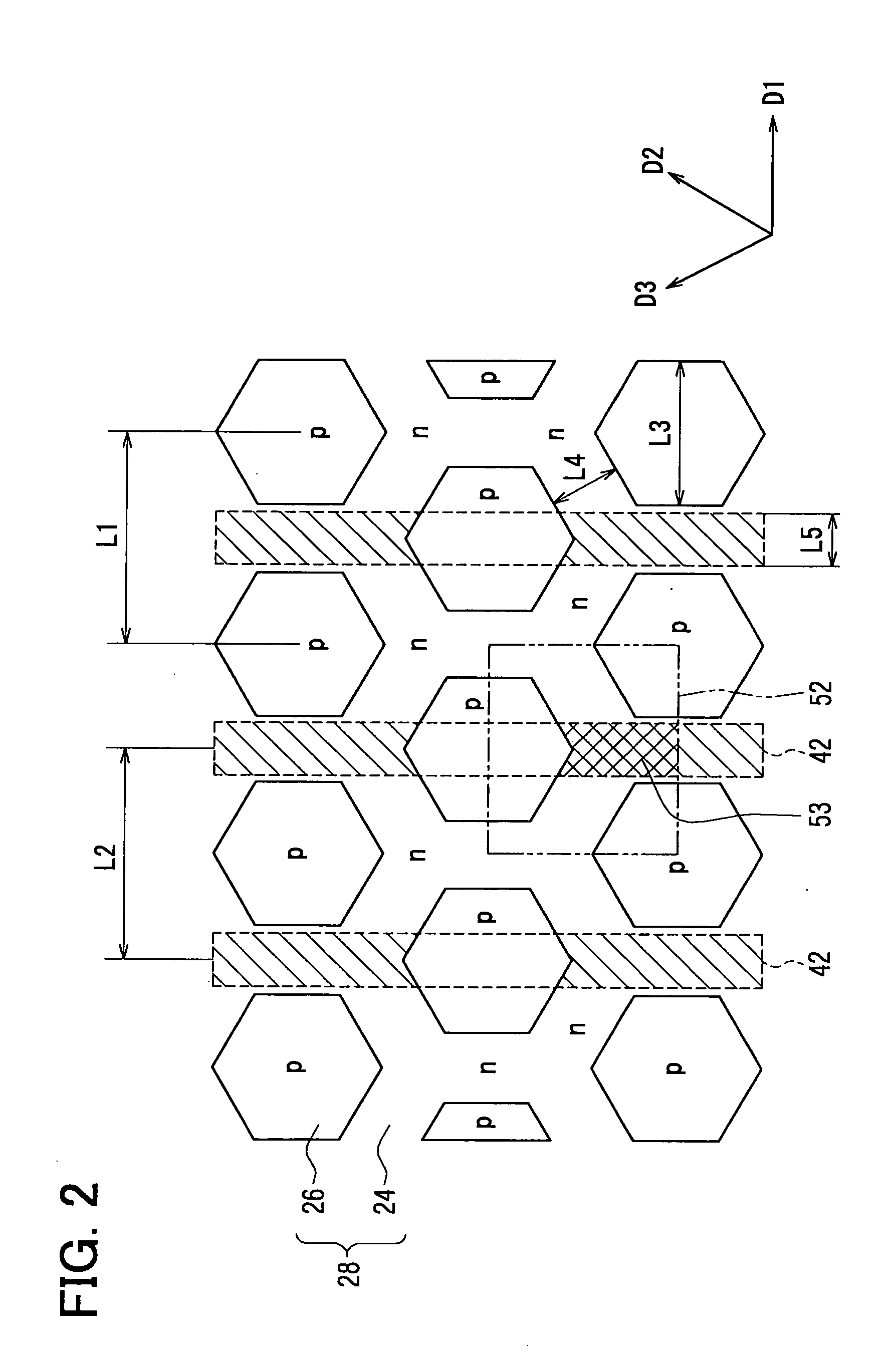
[0069]FIG. 8 is a diagram showing an on-face pattern of p-type columns 26 and n-type columns 24. In the on-face pattern comprising the p-type columns 26 and the n-type columns 24 in accordance with a second embodiment, the p-type columns 26 each having a square cross section are arranged periodically among the n-type columns 24, being distributed in a layout exhibiting regularity. A distance between the gravity points of any adjacent p-type columns 26 is fixed for all the p-type columns 26. A distance L7 between two sides of a p-type column 26, which face each other, is 3 microns. A distance L8 between two adjacent p-type columns 26 is 1 micron. The p-type columns 26 are arranged repetitively on a face perpendicular to a line connecting main electrodes of a main-electrode pair in two directions like directions D1 and D4 shown in the figure.

[0070] A hatched area 42 enclosed by a dashed line shown in FIG. 8 corresponds to the position of each trench gate electrode 42 in the layout. T...

third embodiment

[0080] A third embodiment is an implementation based on results of examining relations between the size of the overlap area and the channel resistance for the first and second embodiments. It is to be noted that these results are results for a 0-degree inclination angle of the trench gate electrode 42. FIG. 13 is a diagram showing relations between the size of the overlap area common to the trench gate electrode 42 and the n-type column 24 versus the channel resistance. In the diagram, the horizontal axis represents the size of the overlap area whereas the vertical area represents the channel resistance.

[0081] The relations shown in FIG. 13 indicate that the size of the overlap area common to the trench gate electrode 42 and the n-type column 24 is proportional to the channel resistance of the semiconductor device. That is, the variation ratio of the size of the overlap area common to the trench gate electrode 42 and the n-type column 24 is approximately equal to the variation rati...


PUM


Abstract

A semiconductor device is fabricated to include a withstand-voltage assurance layer designed into a multi-dimensional super junction structure and a group of trench gate electrodes, each of which penetrating a body layer in contact with the multi-dimensional super junction structure to reach the multi-dimensional super junction structure, so that dispersions of an on-resistance of the semiconductor device can be reduced. When a position at which the group of trench gate electrodes is created is shifted in one direction, the size of an overlap area common to the group of trench gate electrodes and an n-type column changes. However, the group of trench gate electrodes is oriented in such a way that the changes in overlap-area size are minimized.

Description

CROSS REFERENCE TO RELATED APPLICATION [0001] This application is based on and incorporates herein by reference Japanese Patent Application No. 2003-424833 filed on Dec. 22, 2003. FIELD OF THE INVENTION [0002] The present invention relates to a vertical-type semiconductor device having trench gate electrodes and a withstand-voltage assurance layer. More particularly, the present invention relates to a vertical-type semiconductor device having a withstand-voltage assurance layer of a super-junction structure. BACKGROUND OF THE INVENTION [0003] A vertical-type semiconductor device having trench gate electrodes and a withstand-voltage assurance layer is already known. The semiconductor device of this type has a characteristic exhibiting a high withstand voltage and a characteristic exhibiting small on-resistance or a low on-voltage. The on-resistance of the semiconductor device of this type can be considered to be the sum of a drift resistance and a channel resistance. The drift resist...

Claims


Application Information

Patent Timeline
Patent Type & Authority Applications(United States)
IPC IPC(8): G06F17/50H01L27/02H01L29/06H01L29/76H01L29/78
CPCG06F17/5068H01L29/7813H01L29/0634G06F30/39
Inventor KUWAHARA, MAKOTOHATTORI, YOSHIYUKIYAMAUCHI, SHOICHISUZUKI, MIKIMASA
Owner DENSO CORP
Why Eureka
Try Eureka