Manufacturing method of a semiconductor device

a manufacturing method and semiconductor technology, applied in the direction of individual semiconductor device testing, semiconductor/solid-state device testing/measurement, instruments, etc., can solve the problems of low productivity, high cost of semiconductor devices, and high cost of sealing materials, so as to improve the yield in the sealing step of semiconductor devices.

Inactive Publication Date: 2005-06-23
RENESAS ELECTRONICS CORP
View PDF8 Cites 43 Cited by
  • Summary
  • Abstract
  • Description
  • Claims
  • Application Information

AI Technical Summary

Benefits of technology

[0014] It is an object of the present invention to provide a technique able to improve the yield in a sealing step for a semiconductor device which adopts the flip-chip mounting method.
[0017] According to the present invention, when a semiconductor chip mounted on a substrate through protruded electrodes is to be sealed with sealing resin, the internal pressure of a cavity of a molding die is reduced and a substrate clamping pressure of the molding die is changed from a low (weak) pressure to a high (strong) pressure.
[0020] When the semiconductor chip mounted on the substrate through protruded electrodes is to be sealed with resin, the internal pressure of the cavity of the molding die is reduced and the substrate clamping pressure of the molding die is changed from low to high, so that the gap between the semiconductor chip and the substrate can be filled sufficiently with the sealing resin, whereby the yield in the semiconductor device sealing step can be improved.

Problems solved by technology

According to this method, however, since the injection of resin is performed for each semiconductor chip, it takes time for the injection of resin and thus the productivity is low; besides, the resin itself is expensive, resulting in that the cost of the semiconductor device becomes high.
Besides, the cost of the sealing material itself is about one tenths of that in the foregoing known method and is thus much lower.
However, if the above MAP method is adopted in the flip-chip mounting method, since the gap between the semiconductor chip and the wiring substrate is narrow, the sealing resin cannot sufficiently be injected into the gap, thus giving rise to the problem that voids are formed.
If voids are formed due to insufficient injection of the sealing resin into the gap between the semiconductor chip and the wiring substrate, there arise the problem that mutually adjacent bump electrodes melt at the time of heat treatment after the sealing step and are short-circuited through the voids and the problem that the bump electrodes are apt to be disconnected due to deformation of the wiring substrate and a sealing body caused by a temperature cycle after the sealing step.
However, the present inventor has found out that the following problem is involved in the technique of reducing the internal pressure of a molding die cavity when sealing resin in the semiconductor device which adopts the flip-chip mounting method.
In an actual resin sealing step for a semiconductor device which adopts the flip-chip mounting method, even if the interior of a molding die cavity is brought into a state of reduced pressure, sealing resin cannot sufficiently be injected to the back side of the semiconductor chip lying within the cavity, especially into the gap between the semiconductor chip and the wiring substrate used, and voids may occur.
Lead frames are almost constant in thickness, while wiring substrates vary in thickness with an increase in the number of constituent layers, and the range of error is also becoming larger.
As a result, it becomes impossible to let the gas present within the cavity escape sufficiently to the exterior, thus giving rise to the problem that voids are formed.
Especially in the case of the flip-chip mounting method, the problem of voids is apt to occur because the gap between the semiconductor chip and the wiring substrate is very narrow and tends to become still narrower.
On the other hand, if the thickness of the wiring substrate placed within the molding die is smaller than the preset value although it is within the tolerance, the proportion of the crushed portion of the wiring substrate becomes excessively smaller than the preset value, so that the openings of air vents become larger than necessary, with consequent leakage of the sealing resin to the exterior from the air vents.
Once the sealing resin leaks to an outer frame of the wiring substrate, it becomes impossible to effect automatic conveyance, thus giving rise to the problem that the yield and productivity in manufacturing the semiconductor device are deteriorated.

Method used


Image

  • Manufacturing method of a semiconductor device
  • Manufacturing method of a semiconductor device
  • Manufacturing method of a semiconductor device

Examples


first embodiment

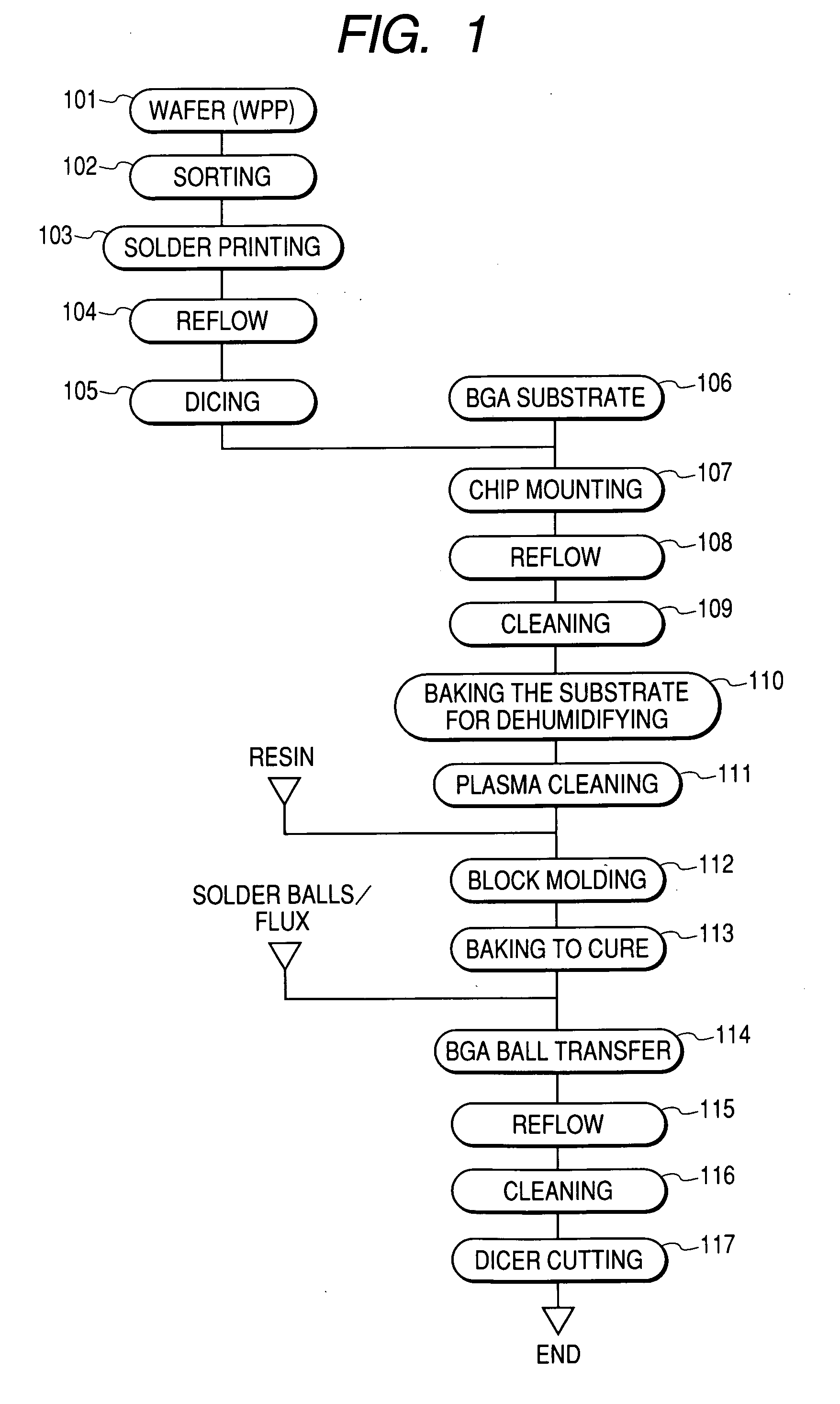
[0068] An example of a semiconductor device manufacturing method according to an embodiment of the present invention will be described below with reference to FIGS. 2 to 24 and in accordance with the process flow shown in FIG. 1.

[0069] First, a description will be given of steps (Steps 101 to 105 in FIG. 1) up to the provision of semiconductor chips (hereinafter referred to simply as “chips”).

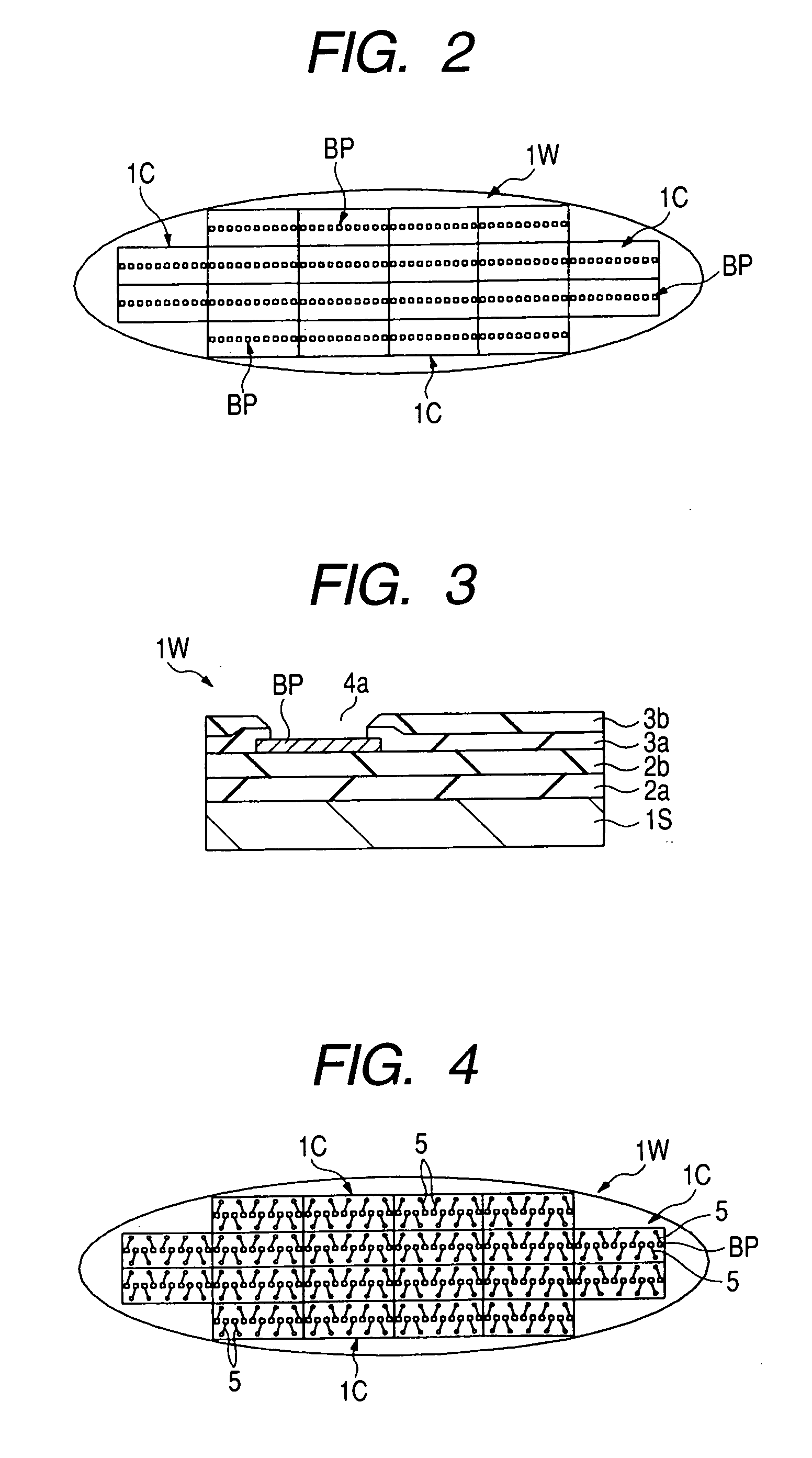
[0070]FIG. 2 is an entire plan view of a wafer 1W after a wafer process. The wafer process, which is also called a pre-process, generally involves such operations as forming elements and wiring layers on a main surface of the wafer 1W having been subjected to mirror polish, forming a surface protecting film, and making it possible to conduct an electrical characteristic test of each of plural chip ICs formed on the wafer 1W, with use of a probe or the like. For example, the wafer 1W is formed in a generally circular shape in plan, and rectangular chip ICs are regularly arranged side by side o...

second embodiment

[0113] In this second embodiment a description will be given about the technique of molding plural chip ICs flip-chip mounted on a substrate matrix 11 with use of a molding die having movable air vents.

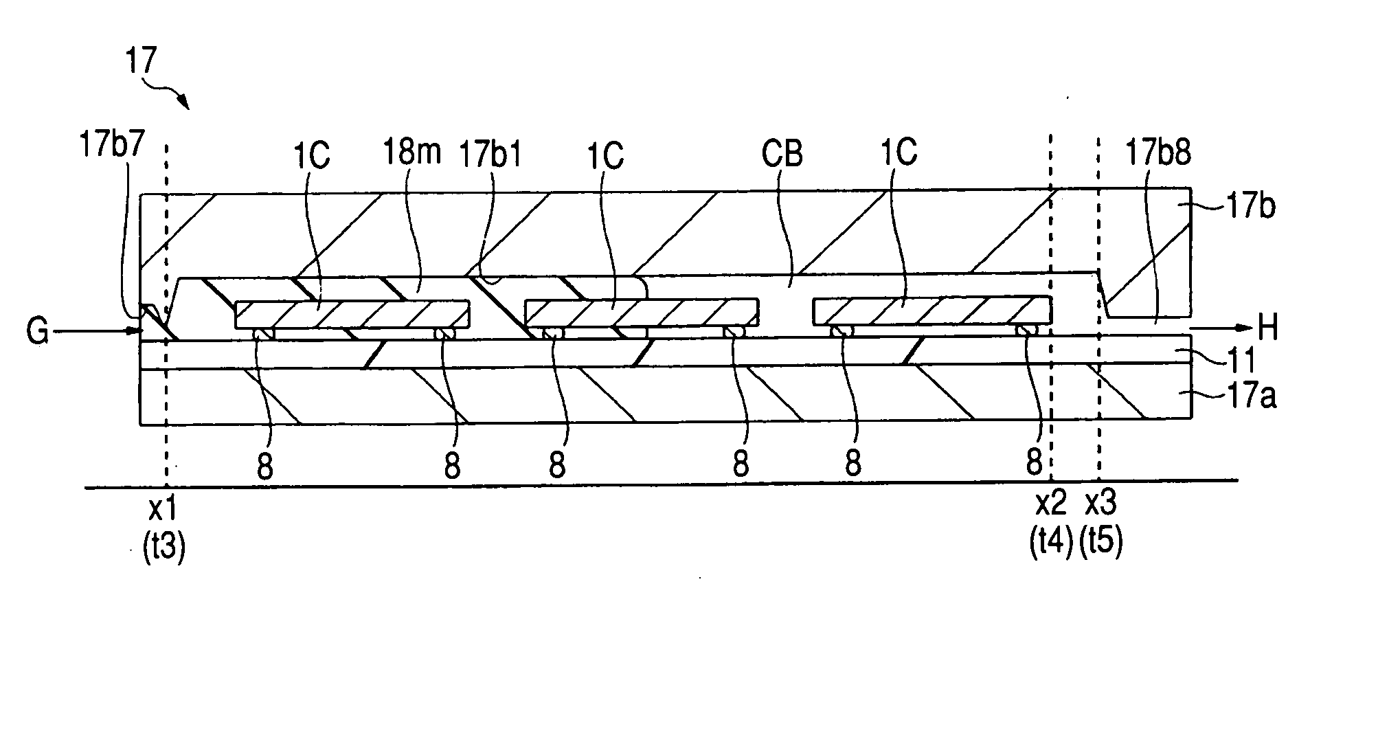
[0114]FIG. 38 is a plan view of a molding apparatus 17 used in this second embodiment, showing a lower die 17a and a lower die 17b in a mutually superimposed state, FIG. 39 is a plan view of a molding surface of the upper die 17b in the molding apparatus 17 shown in FIG. 38, FIG. 40 is a sectional view taken on line J-J in FIG. 38, FIG. 41 is a sectional view taken on line J-J in FIG. 38 in a clamped state of a substrate matrix 11, FIG. 42 is a sectional view taken on line K-K in FIG. 38, FIG. 43 is a sectional view taken on line K-K in FIG. 38 in a clamped state of the substrate matrix 11, and FIG. 44 is an enlarged plan view of a region L shown in FIG. 38. The construction of the lower die 17a in the molding apparatus 17 used in this second embodiment is the same as in the first em...


PUM


Abstract

The yield of a sealing process for a semiconductor device which adopts a flip-chip mounting method is to be improved. In a molding process wherein plural semiconductor chip ICs mounted on a parts mounting surface of a substrate matrix through bump electrodes are to be sealed all together with a sealing resin in a reduced state of the internal pressure of a cavity of a molding apparatus, a clamping pressure at the time of clamping the substrate matrix by both a lower die and an upper die of a molding die is set at a relatively low pressure in an initial stage of injection of the sealing resin and is changed to a relatively high pressure when the sealing resin has covered the semiconductor chip ICs located in a final stage in the resin injecting direction.

Description

CROSS-REFERENCE TO RELATED APPLICATION [0001] The present application claims priority from Japanese patent application No. 2003-424923 filed on Dec. 22, 2003, the content of which is hereby incorporated by reference into this application. BACKGROUND OF THE INVENTION [0002] The present invention relates to a semiconductor device manufacturing method and a semiconductor device technique. Particularly, the present invention is concerned with a technique applicable effectively to a resin sealing technique for a semiconductor device which adopts a flip-chip mounting method. [0003] The flip-chip mounting method is one of mounting methods for mounting a semiconductor chip onto a wiring substrate through bump electrodes (protrude electrodes). In connection with the flip-chip mounting method, as a method for injecting resin into the gap between a semiconductor chip and a wiring board, there is known a method wherein liquid resin is added dropwise to a part of the outer periphery of the semic...

Claims


Application Information

Patent Timeline
Patent Type & Authority Applications(United States)
IPC IPC(8): H01L23/12H01L21/44H01L21/48H01L21/56H01L23/02H01L23/28H01L23/31H01L23/495H01L25/04
CPCH01L21/561H01L2224/16225H01L23/3121H01L24/97H01L2224/16H01L2224/97H01L2924/01013H01L2924/01015H01L2924/01029H01L2924/01033H01L2924/01047H01L2924/01074H01L2924/01075H01L2924/01078H01L2924/01079H01L2924/01082H01L2924/04941H01L2924/04953H01L2924/15311H01L2924/3511H01L21/565H01L2924/014H01L2924/01041H01L2924/01024H01L2924/01005H01L2924/01006H01L2924/01019H01L2224/81H01L24/16H01L2224/023H01L2224/05001H01L2224/05008H01L2224/05022H01L2224/05024H01L2224/05124H01L2224/05144H01L2224/05147H01L2224/05166H01L2224/05171H01L2224/05184H01L2224/05569H01L2224/05572H01L2224/056H01L2224/06131H01L2924/181H01L2924/00H01L2924/00014H01L2924/0001H01L23/02H01L23/28
Inventor UJIIE, KENJIKURATOMI, BUNJI
Owner RENESAS ELECTRONICS CORP
Why Eureka
Try Eureka