
Semiconductor device and method of manufacturing the same

a technology of semiconductor devices and semiconductors, applied in semiconductor devices, semiconductor/solid-state device details, electrical apparatus, etc., can solve the problems of reduced difficult formation of a deep hole, and increased difficulty in embedding metal in association, so as to improve the mechanical improve the yield and reliability of the wiring process, and increase the coupling strength of the connection pillar.

Inactive Publication Date: 2005-06-23
SONY CORP
View PDF15 Cites 3 Cited by
  • Summary
  • Abstract
  • Description
  • Claims
  • Application Information

AI Technical Summary

Benefits of technology

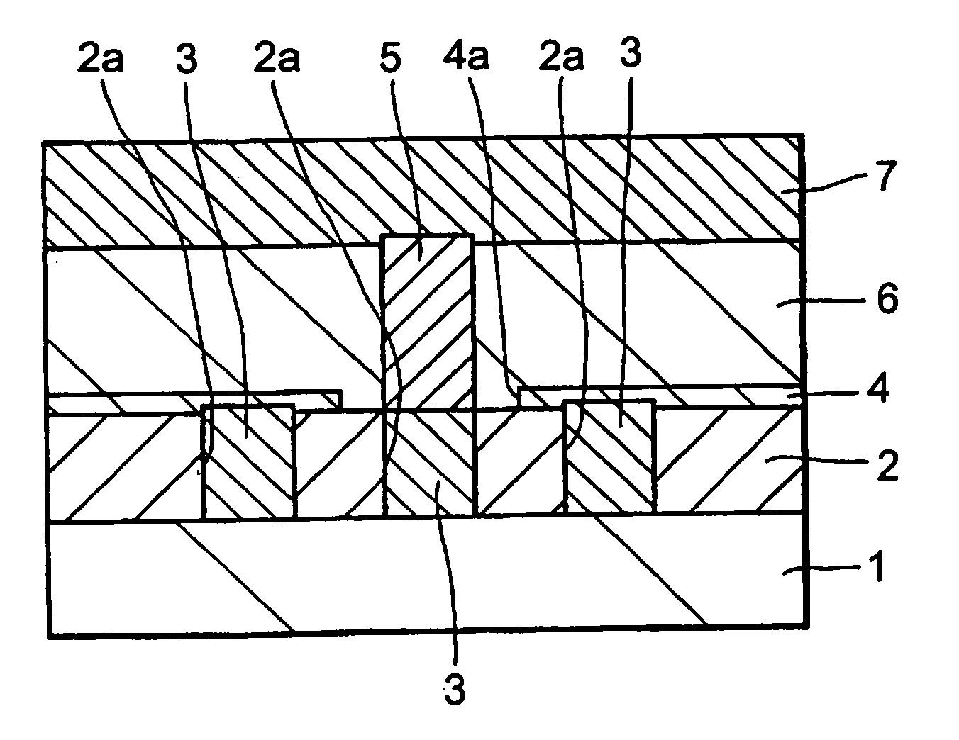
[0024] According to the present invention having the above-mentioned configuration, the connection pillar is formed on the first conductive layer to be self-aligned with respect to this first conductive layer without any usage of the growth guide. That is, it is not necessary to embed the metal in the via hole and the like when forming the connection pillar and to carry out the mask adjustment in the lithography process and the like. Thus, it is possible to avoid the various troubles in association with the embedding operation, the mask adjustment and the like. In addition, the connection pillar can be formed on the first conductive layer in the crystallographically aligned condition. Hence, it is possible to increase the coupling strength of the connection pillar to the first conductive layer and thereby improve the mechanical strength of the connection pillar.
[0025] As mentioned above, according to the present invention, the connection pillar is formed on the first conductive layer, to be self-aligned with respect to the first conductive layer without any usage of the growth guide. Thus, it is possible to avoid the difficulty in the operation for embedding the metal and the problem in association with the embedding operation in the conventional technique. Hence, there occurs no problem of the poisoned via. Also, there occurs no problem of the wiring error resulting from the mask adjustment. Therefore, it is possible to improve the yield and the reliability in the wiring process.

Problems solved by technology

Thus, it is only the alternative technique in the age when the formation of a deep hole was difficult.
However, even if the main technique in the above-mentioned conventional methods of forming the connection pillar continues using a material in Si oxide film system as the interlayer insulation film, it becomes difficult to embed the metal in association with the reduction in a diameter of the via hole and the increase in an aspect ratio of the via hole.
Also, if a base film is required in order to improve the adhesion and grow the film, it is extremely difficult to make the film thickness thinner in proportion to the diameter of the via hole.
This leads to a sharp increase in a wiring resistance of the via hole portion even if a metal of a low resistivity is used.
Moreover, if the interlayer insulation film is replaced by a film of a low dielectric constant, it is difficult to suppress the so-called “poisoned via” (a phenomenon that the defect of the metal embedded by the sputtering method, the CVD method and the like is caused by out-gas from a side wall of the interlayer insulation film) as compared with the case of the usage of the interlayer insulation film in the Si oxide film system.
Also, this technique results in a problem that each time the kind of the film of the low dielectric constant is changed, another suppressing method must be reconsidered.
Also, if the conventional pillar method employs the lift-off method, a lift-off film is limited to resist, and the embedding method is limited to the plating method (thus, a metal such as Al cannot be used by the typical method).
After all, since only the embedded target is different, the above-mentioned problems cannot be solved.
Hence, the defect caused by deviation in the mask adjustments is induced, which brings about a drop in the yield in the wiring process.

Method used


Image

  • Semiconductor device and method of manufacturing the same
  • Semiconductor device and method of manufacturing the same
  • Semiconductor device and method of manufacturing the same

Examples


Embodiment Construction

[0036] An embodiment of the present invention will be described below with reference to the attached drawings. By the way, the same symbols are given to the same or corresponding portions in all the drawings of the embodiment.

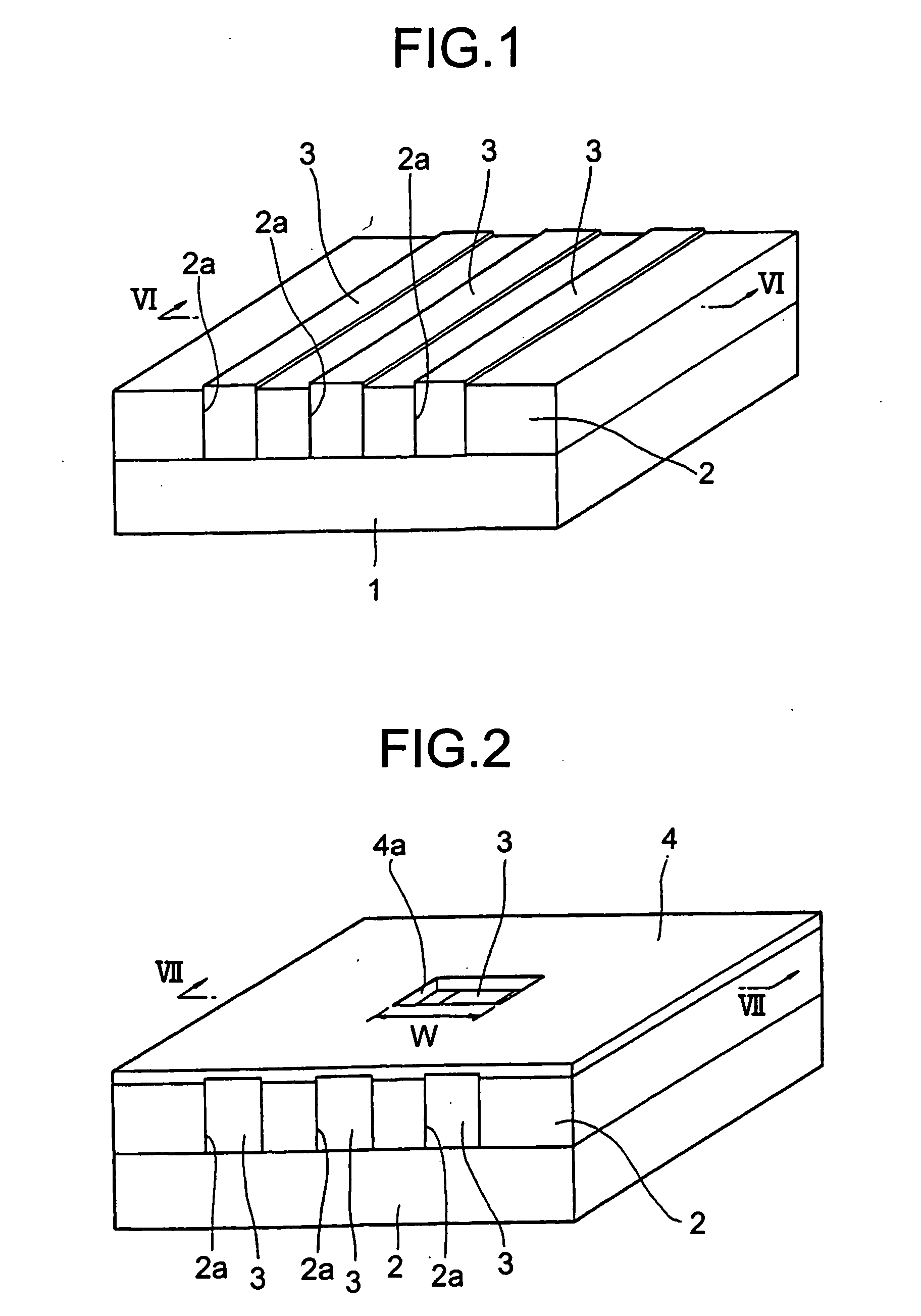
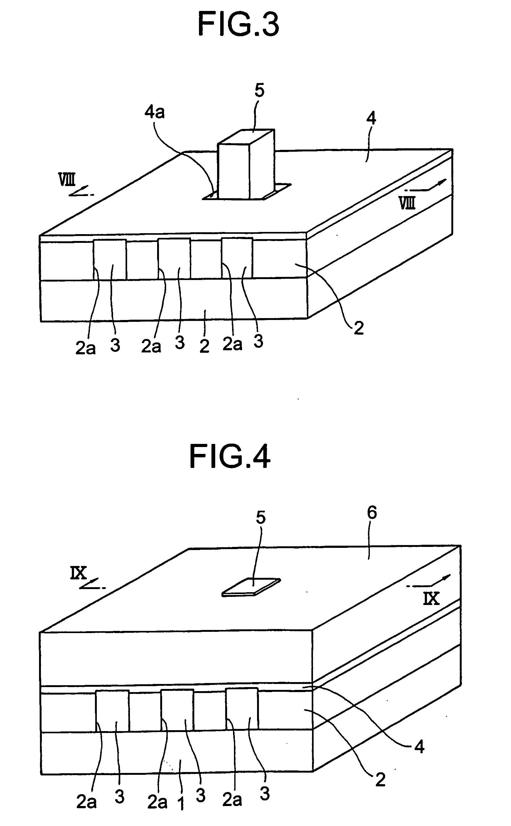
[0037] FIGS. 1 to 5 are the perspective views illustrating a method of manufacturing a semiconductor device according to the embodiment of the present invention, and FIGS. 6 to 10 are the sectional views taken on the respective lines VI-VI to X-X of FIGS. 1 to 5, respectively.

[0038] According to the method of manufacturing the semiconductor device according to this, as shown in FIGS. 1 and 6, an interlayer insulation film 2, for example, such as SiO2 film, and Al wirings 3 being a first layer embedded in grooves 2a formed on the interlayer insulation film 2 are formed on a semiconductor substrate 1 such as an Si substrate on which separation between elements is carried out in advance and on which necessary elements (not shown) such as transistors and the like...


PUM


Abstract

The present invention is to improve yield and reliability in a wiring step of a semiconductor device. When an Al wiring on an upper layer is connected through an connection pillar onto an Al wiring on a lower layer embedded in a groove formed on an interlayer insulation film, a growth suppression film having an opening whose width is wider than that of the Al wiring is formed on the interlayer insulation film and the Al wiring. In this condition, Al and the like are grown by a selective CVD method and the like. Accordingly, the connection pillar is formed on the Al wiring within the opening, in a self-matching manner with respect to the Al wiring.

Description

CROSS REFERENCES TO RELATED APPLICATIONS [0001] The present document is based on Japanese Priority Document JP 2001-052197, filed in the Japanese Patent Office on Feb. 27, 2001, the entire contents of which being incorporated herein by reference. BACKGROUND OF THE INVENTION [0002] 1. Field of the Invention [0003] The present invention relates to a semiconductor device and a method of manufacturing the same. More particularly, it is suitable for an application to a semiconductor device in which a wiring on an upper layer and a wiring on a lower layer are connected to each other through a connection pillar. [0004] 2. Description of Related Art [0005] In a main technique presently being used to connect a wiring on an upper layer and a wiring on a lower layer to each other through a connection pillar in a semiconductor device such as a silicon semiconductor integrated circuit device and the like, an interlayer insulation film is formed for covering the wiring on the lower layer, and a v...

Claims


Application Information

Patent Timeline
Patent Type & Authority Applications(United States)
IPC IPC(8): H01L21/28H01L21/285H01L21/316H01L21/318H01L21/3205H01L21/768H01L23/52H01L23/522H01L23/532
CPCH01L21/28562H01L21/76885H01L23/5226H01L23/53295H01L2924/0002H01L2924/00H01L21/76897
Inventor AOYAMA, JUNICHI
Owner SONY CORP
Learn More