Photonic crystal nano cavity quantum ring single-photon emission device and preparation method thereof

A single-photon emission and photonic crystal technology, applied in the field of quantum information, can solve the problems of difficult to achieve high-performance single-photon emission, unable to cover the 850nm band, small hole energy level separation, etc. Small size and high quantum efficiency

Active Publication Date: 2013-10-09
吉光半导体科技有限公司
View PDF5 Cites 14 Cited by
  • Summary
  • Abstract
  • Description
  • Claims
  • Application Information

AI Technical Summary

Problems solved by technology

However, quantum dot microcavity single photon sources also face many problems, such as: 1) Due to the limitation of the energy band, most of these devices emit light in the 920nm-1300nm band, which cannot cover the 850nm band, and due to the lack of high performance in the >1100nm band The single-photon detectors currently studied mainly focus on the 920-940nm range; 2) the long-wavelength In(Ga)As / GaAs quantum dots have multiple energy levels, and the excitons emit complex light, and the hole energy level separation becomes variable. Very small (8-10meV), the carrier is easily thermalized, the gain is saturated, and it is difficult to achieve high-performance single-photon emission

Method used


Image

  • Photonic crystal nano cavity quantum ring single-photon emission device and preparation method thereof
  • Photonic crystal nano cavity quantum ring single-photon emission device and preparation method thereof
  • Photonic crystal nano cavity quantum ring single-photon emission device and preparation method thereof

Examples


Embodiment 1

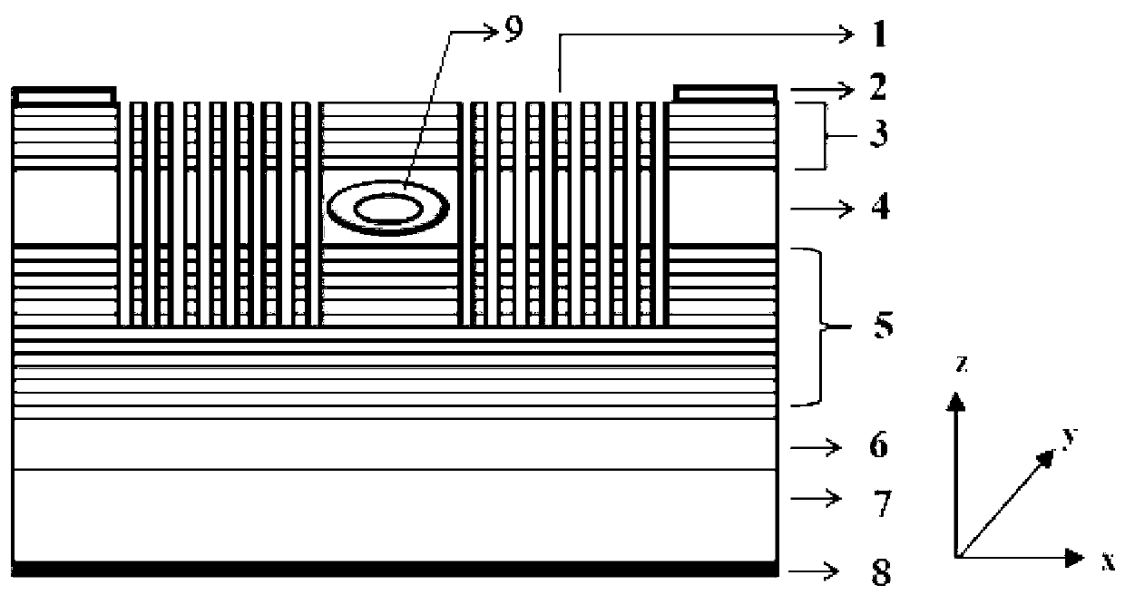
[0038] Taking GaAs / Al(Ga)As quantum ring as an example, the preparation method of the quantum ring is self-organized growth. The specific preparation method of the photonic crystal nanocavity quantum ring single-photon emitting device of the present invention is as follows:

[0039] Step 1: growing 300nm Si-doped GaAs on the n-type highly doped GaAs substrate 7 as the buffer layer 6 with a doping concentration of 2×10 18 cm -3 ; Continue to grow the N-type Bragg reflector 5 on the buffer layer 6, specifically 30 pairs of Al 0.9 Ga 0.1 As and Al 0.1 Ga 0.9 The As material is grown alternately, so that the reflectivity of the N-type Bragg mirror 5 is >95%, and the Si doping concentration is 1×10 18 cm -3 , the thickness of the N-type Bragg reflector 5 is determined according to the condition that the optical thickness of a single layer is 1 / 4 wavelength, that is, nd=1 / 4λ, and the wavelength is the light emitting wavelength of the quantum ring 9;

[0040] Step 2: growing Al...

Embodiment 2

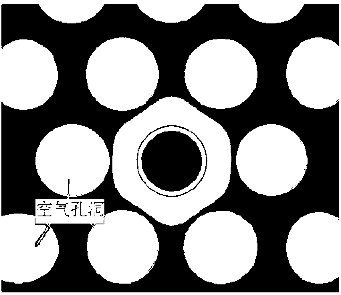
[0048] Taking GaAs / Al(Ga)As quantum rings as an example, the preparation method of the quantum rings can also be prepared by dry etching, and correspondingly, the third step in the method of the present invention is changed to: grow 10nm GaAs, and form a diameter of 30nm by electron beam exposure. A ring with an inner diameter of 10nm, wet etching, a depth of about 10nm, degumming, cleaning, and epitaxial growth of 1 / 4 wavelength Al 0.3 Ga 0.7 As, no doping.


PUM


Abstract

The invention provides a photonic crystal nano cavity quantum ring single-photon emission device and a preparation method of the photonic crystal nano cavity quantum ring single-photon emission device so as to solve the problem that a single photon source exists in a single quantum dot microcavity, and belongs to the field of quantum informatics. A buffer layer, a lower Bragg reflection mirror, an optical flaw layer and an upper Bragg reflection mirror are grown on a substrate in sequence. An upper electrode contact layer is grown on the peripheral zone above the upper Bragg reflection mirror. A lower electrode contact layer is grown below the substrate. A surface transverse two-dimensional photonic crystal structure is formed by an air hole-semiconductor which is manufactured through micro-nano machining. The optical dimension of an internal transverse resonant cavity is half the gain wavelength of a quantum ring. The pattern wavelength of a transverse two-dimensional photonic crystal resonant cavity is matched with the gain wavelength of the quantum ring. The quantum ring is located in the middle of the optical flaw layer and located at the center of a three-dimensional nano cavity formed by the upper Bragg reflection mirror, the lower Bragg reflection mirror and the transverse two-dimensional photonic crystal structure. The quantum ring is used as a light-emitting medium, so that quantum efficiency is higher. The quantum ring material can cover a wave band which cannot be covered by quantum dots.

Description

technical field [0001] The invention relates to a photonic crystal nanocavity quantum ring single-photon emitting device and a preparation method thereof, belonging to the technical field of quantum information. Background technique [0002] The single photon source is the key component to realize the single photon qubit, optical quantum key transmission, optical quantum computing and quantum network. It will bring new changes to the transmission and processing of information by human beings. From the perspective of application, if it is applied to quantum communication, the ideal single photon source should be electrically driven, work at room temperature, work in the communication band (850nm, 1310nm and 1550nm), high single photon emission efficiency, high clock frequency, if If it is used for optical quantum computing, it is more hoped that it can be integrated. [0003] There are many ways to generate single photons, such as laser attenuation, nonlinear medium paramet...

Claims


Application Information

Patent Timeline
Patent Type & Authority Applications(China)
IPC IPC(8): H01S5/125H01S5/343
Inventor 佟存柱田思聪汪丽杰邢恩博王立军
Owner 吉光半导体科技有限公司
Why Eureka
Try Eureka