Preparation method of surface-enhanced Raman scattering substrate of metal particle array
A surface-enhanced Raman and metal particle technology, applied in Raman scattering, material excitation analysis, etc., can solve problems such as easy oxidation, poor time stability, etc.
- Summary
- Abstract
- Description
- Claims
- Application Information
AI Technical Summary
Problems solved by technology
Method used
Image
Examples
Embodiment 1
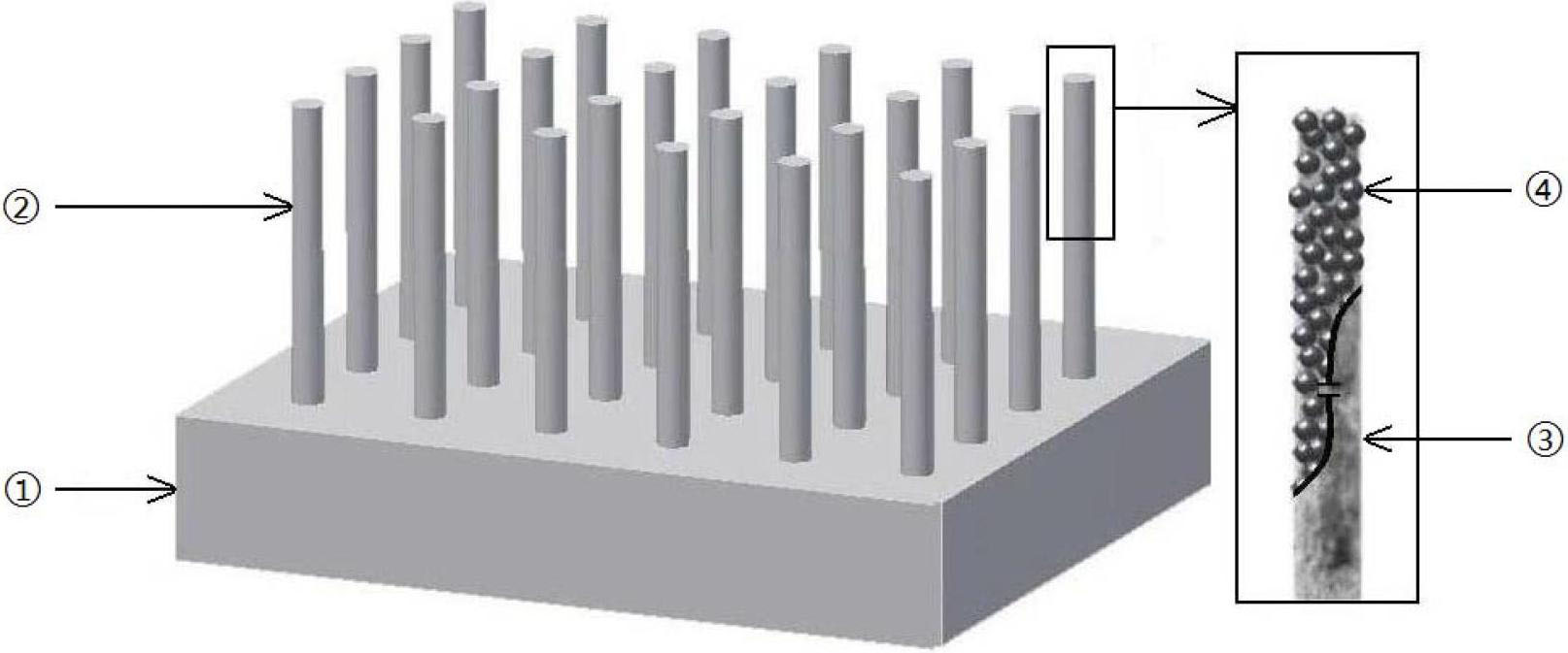
[0017] (1) Place an n or p-type single crystal silicon wafer with a resistivity of 2 Ω?cm in the reactor, and fill it with 10% HF and 0.005mol / L AgNO 3 and H with a mass fraction of 0.5% 2 o 2 The composition of the etching solution, the solution volume filling degree of the reaction kettle is 80%, and it is etched at a temperature of 50°C for 15 minutes. After the above-mentioned metal-assisted chemical etching method, the porous silicon nanowire array of the substrate material required for the substrate can be prepared. ;
[0018] (2) Put the porous silicon nanowire array in 0.01mol / L AgNO 3 Immerse in the solution for 2 minutes, remove and wash with N 2 Blow dry to obtain the metal particle array-based surface-enhanced Raman scattering substrate;
[0019] (3) Drop the rhodamine 6G solution onto the surface of the substrate in the form of a hanging drop, put it into a Raman spectrometer for analysis, and the detection limit can be as low as 10 -16 mol / L.
Embodiment 2
[0021] (1) Place an n-type (111) oriented monocrystalline silicon wafer with a resistivity of 0.001Ω·cm in a reactor, and fill it with 1% HF and 0.001mol / L AgNO 3 and H with a mass fraction of 0.1% 2 o 2 The composition of the etching solution, the solution volume filling degree of the reaction kettle is 40%, and it is etched at a temperature of 10°C for 2 hours. After the above-mentioned metal-assisted chemical etching method, the porous silicon nanowire array of the substrate material required for the substrate can be prepared. ;
[0022] (2) Put the porous silicon nanowire array in 40% HF and 1mol / L AgNO 3 After immersing in the mixed solution for 1 second, take it out and dry it naturally to obtain a metal particle array-based surface-enhanced Raman scattering substrate;
[0023] (3) Drop the pesticide Thiram solution onto the surface of the substrate in the form of hanging drops, put it into a Raman spectrometer for analysis, and the detection limit can be as low as 10...
Embodiment 3
[0025] (1) A p-type (100) oriented single crystal silicon wafer with a resistivity of 50 Ω cm was placed in a reactor, filled with 40% HF and 1mol / L AgNO 3 and H with a mass fraction of 10% 2 o 2 The composition of the etching solution, the solution volume filling degree of the reaction kettle is 90%, and it is etched at a temperature of 100 ° C for 1 minute. After the above-mentioned metal-assisted chemical etching method, the porous silicon nanowire array of the substrate material required for the substrate can be prepared. ;
[0026] (2) Put the porous silicon nanowire array in 0.0001mol / L HAuCl 4 Immerse in the solution for 1 hour, take it out and wash it in N 2 Blow-dry in medium to obtain the metal particle array-based surface-enhanced Raman scattering substrate;
[0027] (3) Soak the substrate in Rhodamine 6G solution for 1 hour, take it out, dry it, put it into a Raman spectrometer for analysis, the detection limit can be as low as 10 -12 mol / L.
PUM
| Property | Measurement | Unit |
|---|---|---|
| quality score | aaaaa | aaaaa |
Abstract
Description
Claims
Application Information

