Method of doping organic semiconductors with quinone derivatives and 1, 3, 2 - dioxaborine derivatives

a technology of organic semiconductors and dioxaborine, which is applied in the direction of non-metal conductors, sustainable manufacturing/processing, final product manufacturing, etc., can solve the problems of high control and regulation expenses, inability to precisely control the manufacturing process in large technical production plants or those on a technical scale, and disadvantages of compounds previously investigated, so as to facilitate the processing of organic semiconductors and reduce volatility

Inactive Publication Date: 2005-06-30
KUEHL OLAF +4
View PDF1 Cites 457 Cited by
  • Summary
  • Abstract
  • Description
  • Claims
  • Application Information

AI Technical Summary

Problems solved by technology

However, the compounds previously investigated have disadvantages for technical use in the production of doped semiconducting organic layers or of suitable electronic components with doped layers of this kind.
The manufacturing processes in large technical production plants or those on a technical scale cannot always be precisely controlled, requiring high control and regulation expenses during processing in order to obtain the desired product quality, or to undesirable tolerances of the products.
In addition, there are disadvantages associated with the use of previously known organic donors with regard to electronic component structures, such as light-emitting diodes (OLEDs), field-effect transistors (FETs) or solar cells themselves due to production difficulties related to handling of dopants.
The electronic components may exhibit undesirable heterogeneities or the electronic components may exhibit undesirable aging effects.

Method used


Image

  • Method of doping organic semiconductors with quinone derivatives and 1, 3, 2 - dioxaborine derivatives
  • Method of doping organic semiconductors with quinone derivatives and 1, 3, 2 - dioxaborine derivatives
  • Method of doping organic semiconductors with quinone derivatives and 1, 3, 2 - dioxaborine derivatives

Examples


example 1

[0389] Doping of ZnPc with N,N′-dicyano-2,3,5,6-tetrafluoro-1,4-quinonediimine (F4DCNQI)

[0390] The evaporation temperature T(evap.) is 85° C. The two components matrix and dopant were deposited from vapor under vacuum in a ratio of 50:1. Here the conductivity is 2.4×10⁻² s / cm. Results are shown in FIG. 1 and Table 1 below.

TABLE 1Layer ThicknessCurrent(nm)(nA)569.0510400.915762.5201147251503.2301874.4352233.4402618453001.5503427

example 2

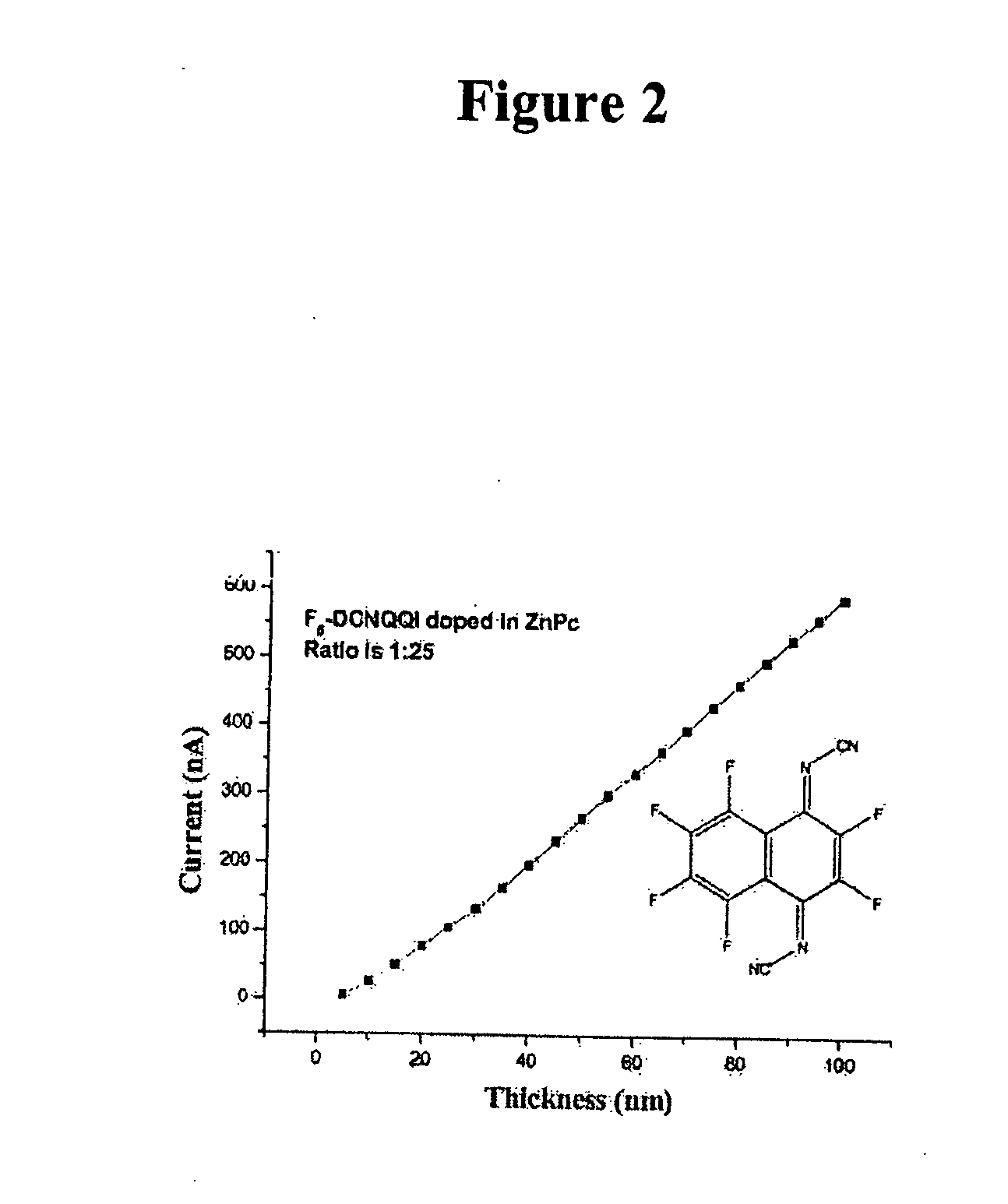
[0391] Doping of ZnPc with N,N′-dicyan-2,5-dichloro-1,4-quinonediimine (C12DCNQI) the evaporation temperature T(evap.) is 114° C. The ratio of the two compounds in the vapor-deposited layer is 1:50 in favor of the matrix. A conductivity of 1.0×10⁻² s / cm was measured in the layer. Results are shown in FIG. 2 and Table 2 below.

TABLE 2Layer ThicknessCurrent(nm)(nA)542.6610179.415334.22048425635.53078635946401091.5451253501409.8

example 3

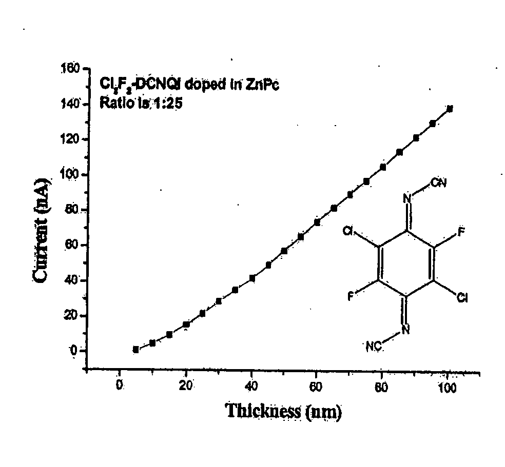
[0392] Doping of ZnPc with N,N′-dicyano-2,5-dichloro-3,6-difluoro-1,4-quinonediimine (C12F2DCNQI)

[0393] The evaporation temperature T(evap.) is 118° C. The layer was vapor-deposited under vacuum at the ratio of 1:25 (dopant matrix). A conductivity of 4.9×10⁻⁴ s / cm was measured there. Results are shown in FIG. 3 and Table 3 below.

TABLE 3LayerthicknessCurrent(nm)(nA)51.1648104.7852159.72112015.5822521.9853028.8663535.454042.2494549.7475057.865566.0126074.3356582.4497090.2517597.96880106.1485114.5890122.8495131.1100139.59


PUM

PropertyMeasurementUnit
pressureaaaaaaaaaa
temperatureaaaaaaaaaa

Abstract

The invention relates to the use of an organic mesomeric compound as organic dopant for doping an organic semiconducting matrix material for varying the electrical properties thereof. In order to be able to handle organic semiconductors more easily in the production process and to be able to produce electronic components with doped organic semiconductors more reproducibly, a quinone or quinone derivative or a 1,3,2-dioxaborine or a 1,3,2-dioxaborine derivative may be used as a mesomeric compound, which under like evaporation conditions has a lower volatility than tetrafluorotetracyanoquinonedimethane (F4TCNQ).

Description

CROSS-REFERENCE TO RELATED APPLICATIONS [0001] The present application is a continuation application of U.S. patent application Ser. No. 10 / 792,133, filed Mar. 3, 2004, which claimed priority to German Patent Application No. 103 57 044.6, filed Dec. 4, 2003, both of which are incorporated herein by reference in their entirety.BACKGROUND OF THE INVENTION [0002] The invention relates to the use of an organic mesomeric compound as an organic dopant for doping an organic semiconducting matrix material for varying the electrical properties thereof, a doped semiconducting matrix material, and an electronic component made of the latter. [0003] The doping of silicon semiconductors has already been state of art for several decades. By this method, an increase in conductivity, initially quite low, is obtained by generation of charge carriers in the material as well as, depending upon the type of dopant used, a variation in the Fermi level of the semiconductor. [0004] However, several years ag...

Claims


Application Information

Patent Timeline
Patent Type & Authority Applications(United States)
IPC IPC(8): H01L51/50A61K31/53C07C251/22C07D339/08C07F5/04C09K11/06H01L21/04H01L21/24H01L29/786H01L29/861H01L31/00H01L35/24H01L51/00H01L51/05H01L51/30H01L51/40H01L51/54H05B33/14
CPCC09K11/06Y02E10/549C09K2211/1011C09K2211/1092H01L51/001H01L51/002H01L51/0051H01L51/0052H01L51/0054H01L51/0059H01L51/0067H01L51/007H01L51/0071H01L51/0072H01L51/0074H01L51/0078H01L51/0079H01L51/008H01L51/0092H01L51/5052Y02B10/10C09B69/102C09B69/105C09B69/109C09K2211/1007Y02P70/50H10K71/164H10K71/30H10K85/611H10K85/622H10K85/615H10K85/6565H10K85/631H10K85/654H10K85/321H10K85/6576H10K85/657H10K85/6572H10K85/311H10K85/322H10K85/381H10K50/155H01L21/24
Inventor KUEHL, OLAFHARTMANN, HORSTZEIKA, OLAFPFEIFFER, MARTINYOUXUAN, ZHENG
Owner KUEHL OLAF
Why Eureka
Try Eureka