
Image sensor

a technology of image sensor and microlens array, which is applied in the field of image sensor, can solve the problems of high process cost of ccds, high driving voltage, and general requirement of additional supporting circuits, and achieve the effects of avoiding or reducing the damage to the microlens array, and maintaining the quality of the image reproduced by the image sensor

Inactive Publication Date: 2005-06-30
DONGBU ELECTRONICS CO LTD
View PDF14 Cites 15 Cited by
  • Summary
  • Abstract
  • Description
  • Claims
  • Application Information

AI Technical Summary

Benefits of technology

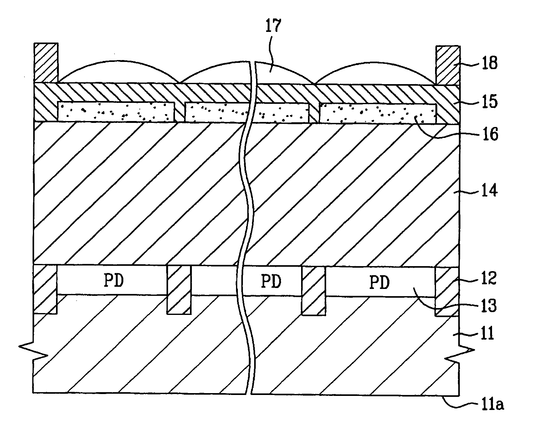
[0013] An object of the present invention is to provide an image sensor, in which a light shielding layer is shifted to or located in a circumference of the microlens array, and a thickness of the light shielding layer is greater than a thickness of the microlens array, to prevent a contaminant blocking sealing tape from being brought into direct contact with the microlens array. The supporting action of the light shielding layer is believed to avoid or reduce damage to the microlens array, even if a pressure is applied to the microlens array to press the sealing tape strongly during polishing of a back surface of the semiconductor substrate.
[0014] Another object of the present invention is to provide an image sensor, in which damage to a microlens array which may result from polishing of a back surface of a semiconductor substrate and inadvertent contact with a sealing tape is prevented, to maintain or optimize a light converging function of the microlens array and / or substantially improve or maintain a quality of the image reproduced by the image sensor.
[0016] To achieve these objects and other advantages and in accordance with the purpose of the invention, as embodied and broadly described herein, an image sensor includes a microlens array for converging an external light incident thereon, an optional color filter array for converting the light converged by the microlens array into a color light, a photodiode array on a semiconductor substrate at an active region, for receiving the light converged by the microlens array and to produce and store photo charges, an optional light transmission layer over the semiconductor substrate to cover the photodiode array, to support the microlens array and the (optional) color filter array, and to transmit the light converged by the microlens array toward the photodiode array, and a light shielding support layer at a circumference of the microlens array, adapted to shield an external light, support an external particle shielding tape if attached, and prevent or inhibit the microlens array from being brought into physical contact with the tape.

Problems solved by technology

However, the CCD has many disadvantages, such as a high driving voltage, and an additional separate supporting circuit is generally required.
Thus, the process cost for CCDs is high, and as a result, the present trend in the use of the CCD is decreasing.
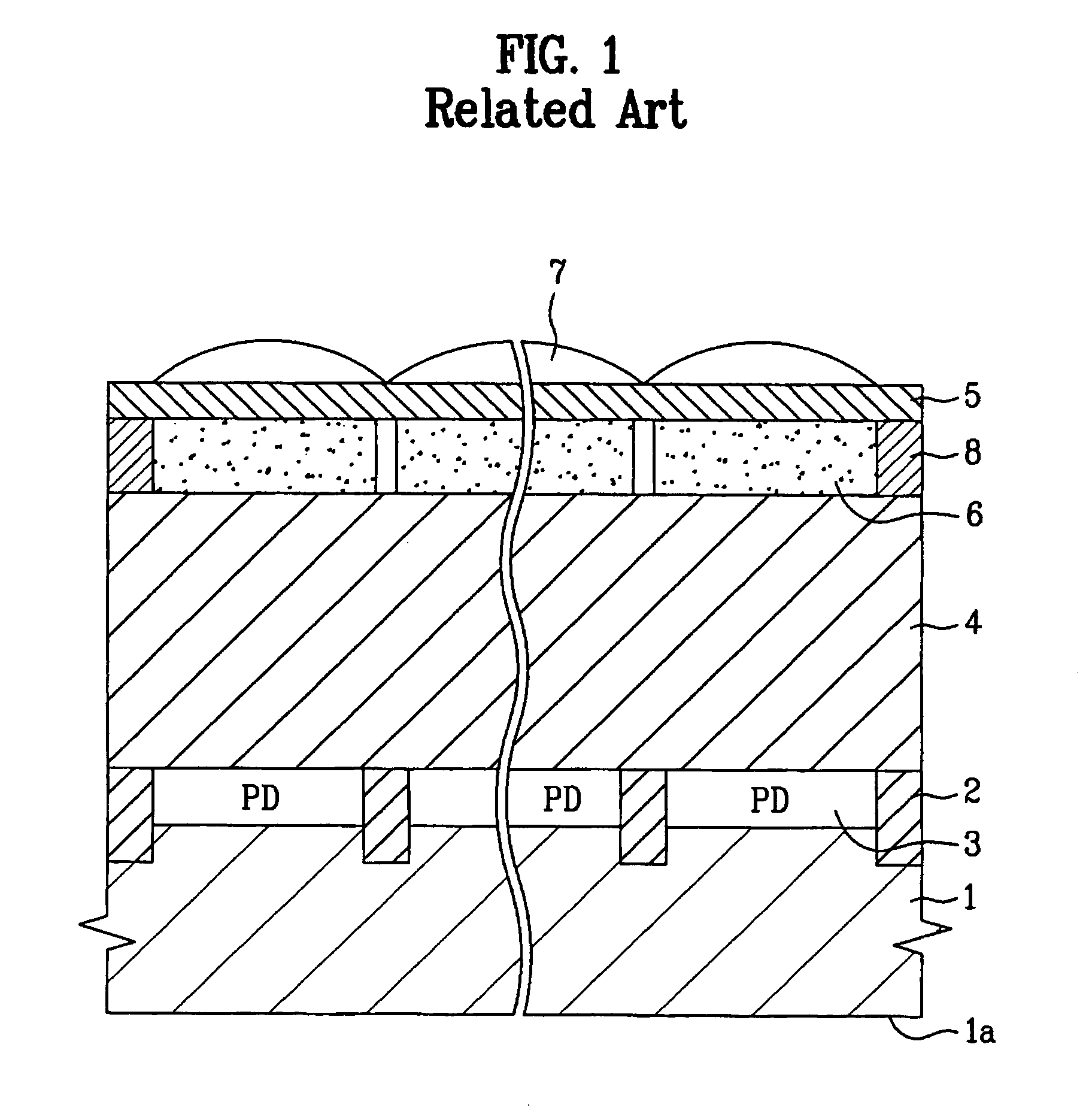
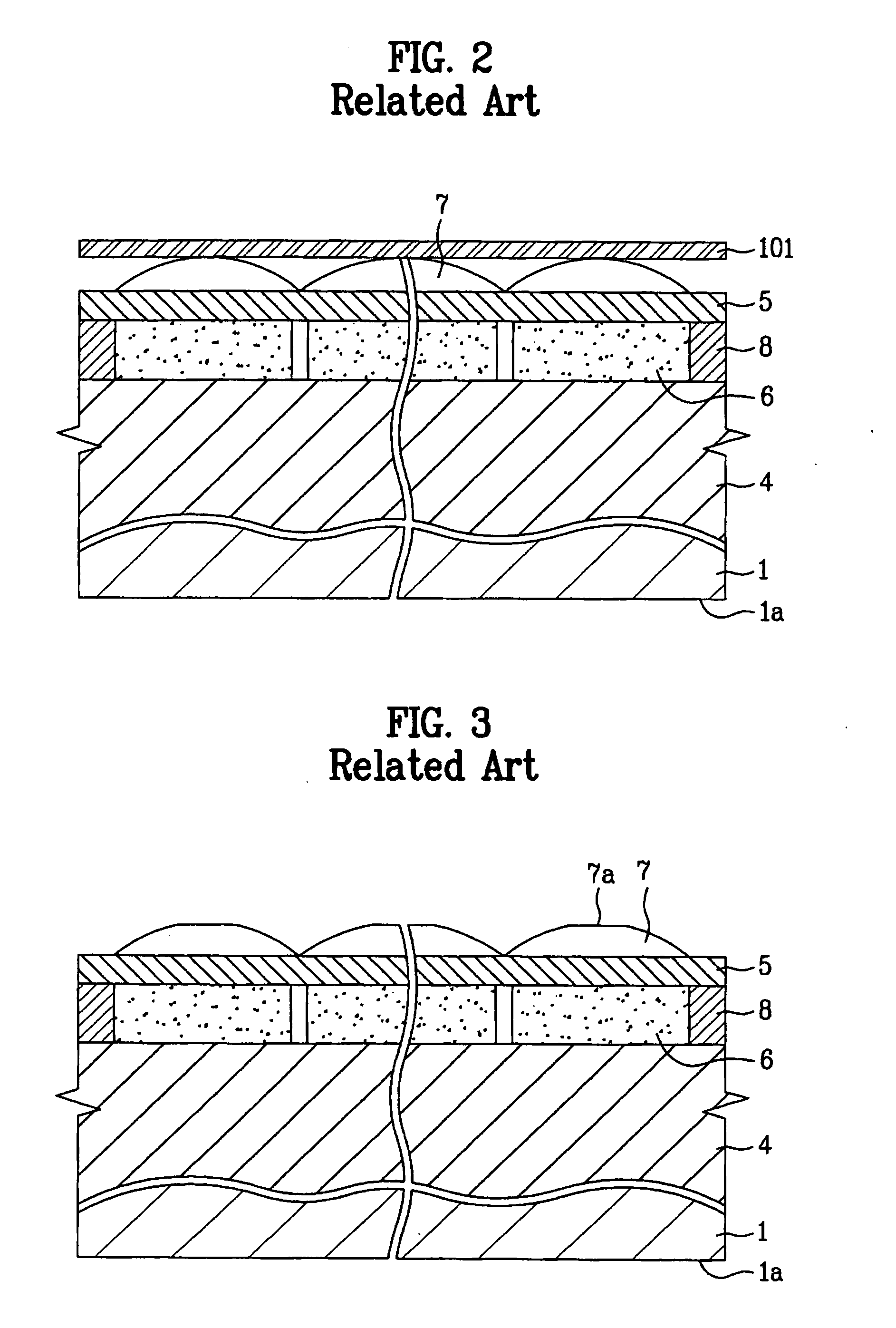
However, the polishing inevitably produces many silicon particles from the back surface 1a of the semiconductor substrate, which move toward a surface of the semiconductor substrate 1 due to static electricity generated during the spin polishing, resulting in contamination of various structures on the image sensor.
Of course, if the curvature damaged surface 7a is left as it is without taking any measures, the microlens array 7 fails to perform a regular light converging function, leading to an image reproduction of which quality is poor.

Method used


Image

  • Image sensor
  • Image sensor
  • Image sensor

Examples


Embodiment Construction

[0025] Reference will now be made in detail to the preferred embodiments of the present invention, examples of which are illustrated in the accompanying drawings. Wherever possible, the same reference numbers will be used throughout the drawings to refer to the same or like parts.

[0026] Referring to FIG. 4, the image sensor, for an example, a CMOS image sensor, includes a microlens array 17 for converging an external light incident thereon, a color filter array 16 for converting the light converged by the microlens array 17 into a color light, a light transmission layer 14 for transmission of the light converted into the color light at the color filter layer 17 toward a photodiode array 13, and the photodiode array 13 on an active region of a semiconductor substrate 11 defined by an active cell isolation layer 12, for receiving the light passed through the light transmission layer 14 and producing and storing photo charges. The light transmission layer 14 is formed over the semicon...


PUM


Abstract

An image sensor is disclosed, in which a light shielding layer is positioned in a circumference of a microlens array, and the light shielding layer has a thickness greater than that of the microlens array, to prevent a contaminant blocking sealing tape from directly contacting the microlens array and support the sealing tape, thereby avoiding damage to the microlens array when pressure is applied to press the sealing tape and / or polish a back surface of a semiconductor substrate. If such damage is prevented, the light converging function of the microlens array may be optimized, and the quality of the image reproduced by the image sensor can also be improved, substantially.

Description

CROSS-REFERENCE TO RELATED APPLICATIONS [0001] This application claims the benefit of Korean Application No. P2003-0098107 filed on Dec. 27, 2003, which is hereby incorporated by reference as if fully set forth herein. BACKGROUND OF THE INVENTION [0002] 1. Field of the Invention [0003] The present invention relates to image sensors, and more particularly, to an image sensor in which a light shielding layer is shifted to or located in a circumference of a microlens array, and a thickness of the light shielding layer is greater than a thickness of the microlens array, to prevent a contaminant blocking sealing tape from being brought into direct contact with the microlens array in advance by supporting action of the light shielding layer, and for reducing or avoiding damage to the microlens array easily, for example when a pressure is conventionally applied to the microlens array to press the sealing tape strongly, or during polishing of a back surface of a semiconductor substrate. [00...

Claims


Application Information

Patent Timeline
Patent Type & Authority Applications(United States)
IPC IPC(8): G02B17/00H01L27/146H01L31/10
CPCH01L27/14618H01L27/14685H01L27/14627H01L27/14623H01L2924/0002H01L2924/00H01L27/146H01L31/10
Inventor HONG, CHANG YOUNG
Owner DONGBU ELECTRONICS CO LTD
Learn More