Eureka AIR delivers breakthrough ideas for toughest innovation challenges, trusted by R&D personnel around the world.

Trench isolation method in flash memory device

Active Publication Date: 2005-06-30
MARVELL ASIA PTE LTD +1
View PDF5 Cites 4 Cited by
  • Summary
  • Abstract
  • Description
  • Claims
  • Application Information

AI Technical Summary

Benefits of technology

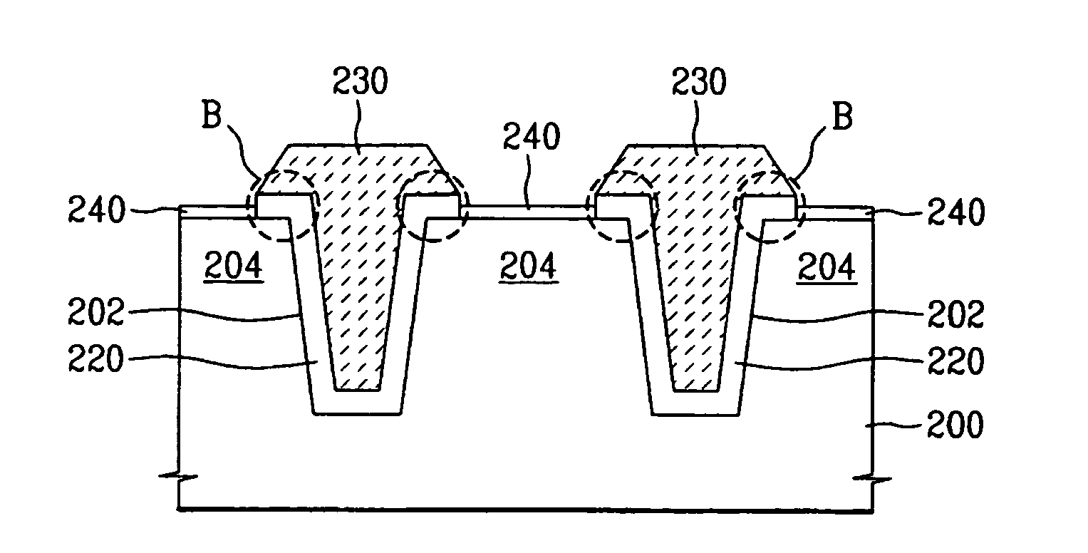
[0017] An object of the present invention is to provide a trench isolation method in a flash memory device, by which stability and reliability of the device are enhanced in a manner of forming a pad oxide layer thick in the vicinity of an edge of a trench isolation layer.

Problems solved by technology

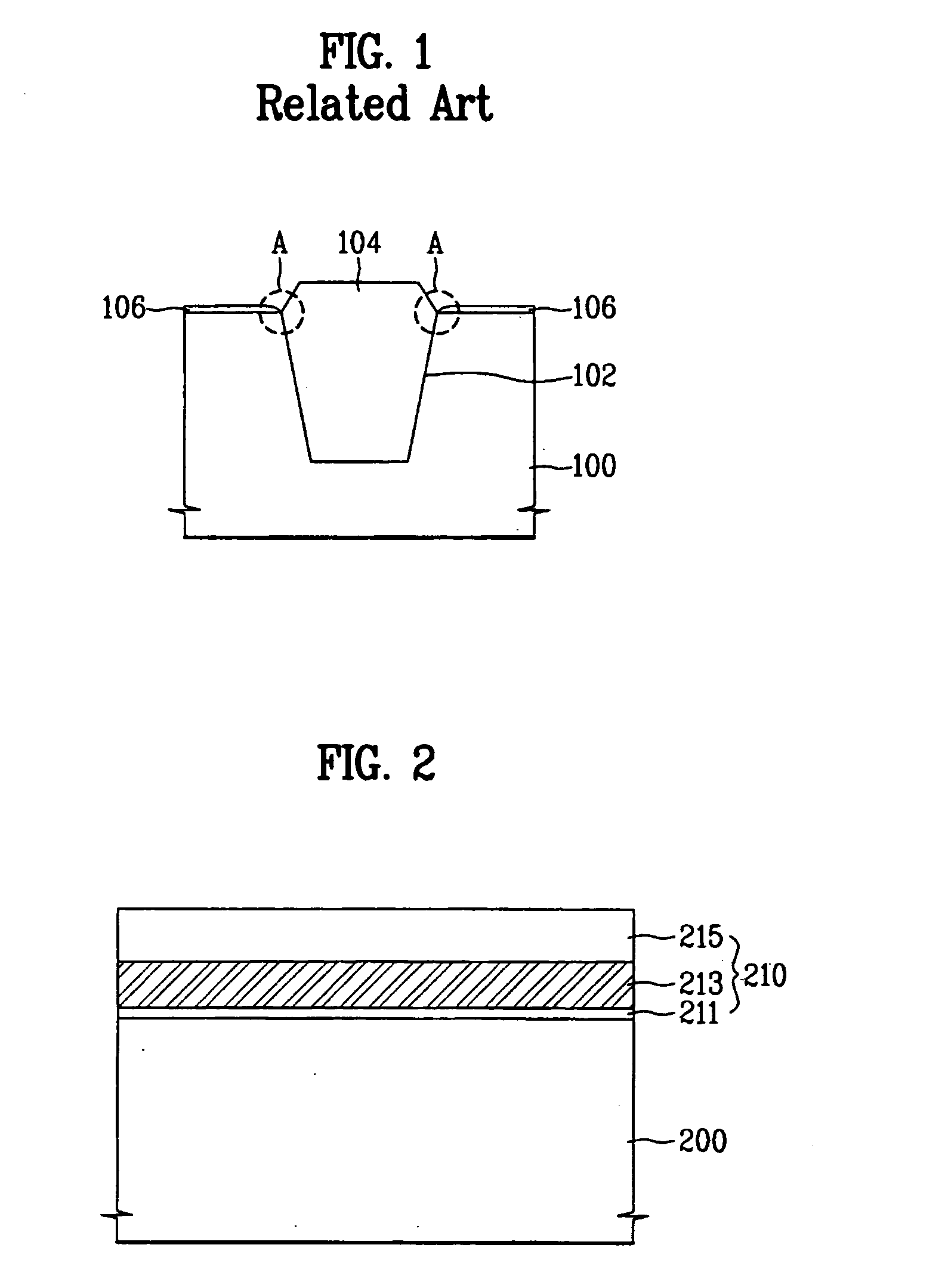
Specifically, since an electric field is intensively focused on the edge A of the trench isolation layer 104, the uneven configuration of the pad oxide layer 106 degrades stability and reliability of the device.

Method used


Image

  • Trench isolation method in flash memory device
  • Trench isolation method in flash memory device
  • Trench isolation method in flash memory device

Examples


Embodiment Construction

[0031] Reference will now be made in detail to the preferred embodiments of the present invention, examples of which are illustrated in the accompanying drawings. Wherever possible, the same reference numbers will be used throughout the drawings to refer to the same or like parts.

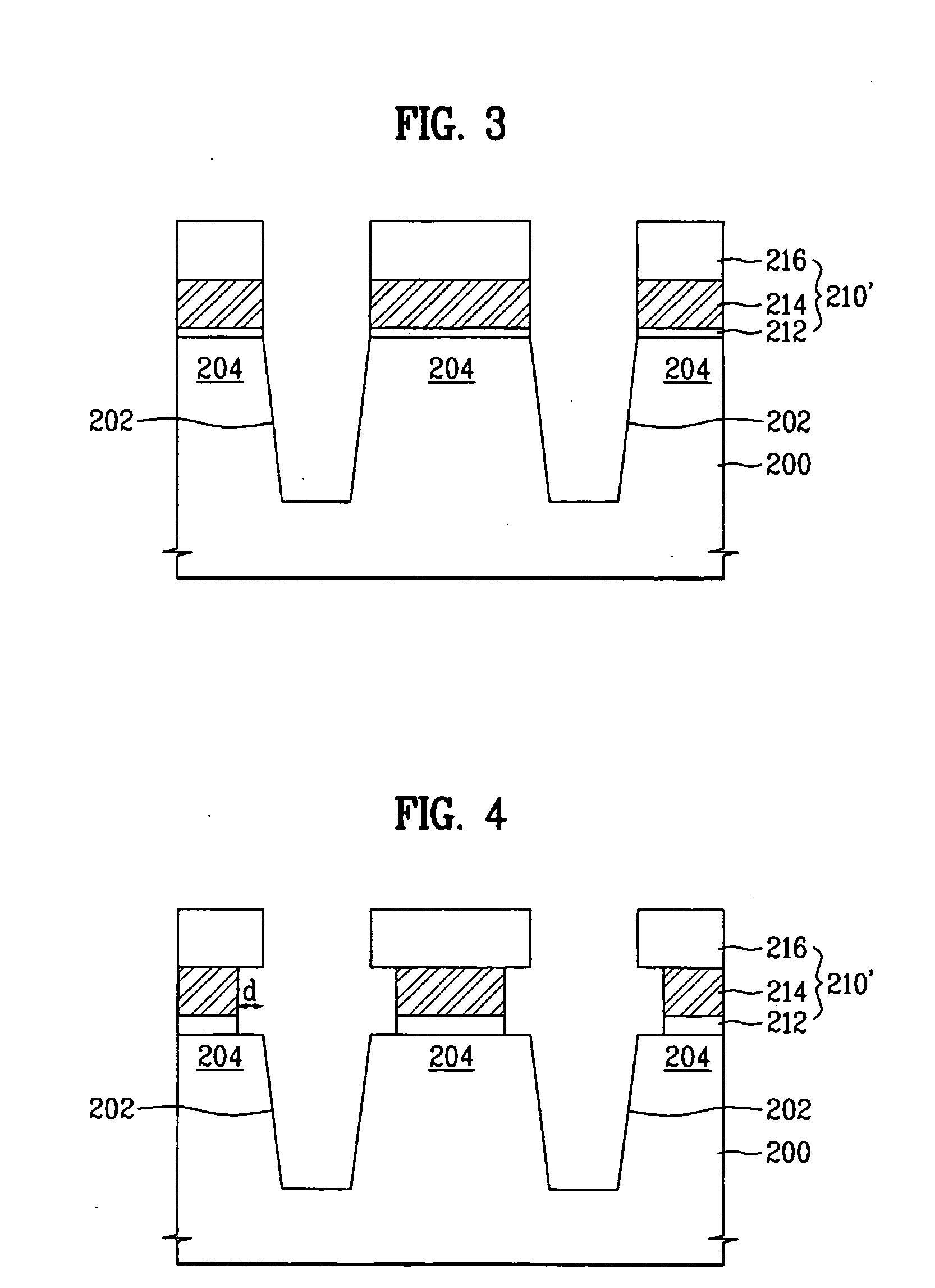
[0032] FIGS. 2 to 6 are cross-sectional diagrams for explaining a method of forming a trench isolation layer in a flash memory device according to the present invention.

[0033] Referring to FIG. 2, a pad oxide layer 211, a nitride layer 213, and a TEOS oxide layer 215 are sequentially stacked on a semiconductor substrate 200, e.g., silicon substrate to configure a mask layer 210. The mask layer 210 is provided for trench etch. Specifically, the nitride layer 213 will be used as an etch stop layer in per forming planarization later.

[0034] Referring to FIG. 3, a photoresist pattern (not shown in the drawing) is formed on the mask layer 210 in FIG. 2 to define a device isolation area over the silicon substra...


PUM


Abstract

The present invention provides a trench isolation method in a flash memory device, by which stability and reliability of the device are enhanced in a manner of forming a pad oxide layer thick in the vicinity of an edge of a trench isolation layer. The present invention includes forming a mask layer pattern on a semiconductor substrate to expose a device isolation area but to cover an active area thereof, the mask layer pattern comprising a first insulating layer pattern and a second insulating layer pattern stacked thereon, forming a trench in the semiconductor substrate corresponding to the device isolation area, removing an exposed portion of the first insulating layer pattern enough to expose a portion of the semiconductor substrate in the active area adjacent to the trench, forming a sidewall oxide layer on an inside of the trench and the exposed portion of the semiconductor substrate, filling up the trench with a third insulating layer to cover the sidewall oxide layer, and removing the mask layer pattern.

Description

[0001] This application claims the benefit of the Korean Application No. P2003-0098367 filed on Dec. 27, 2003, which is hereby incorporated by reference. BACKGROUND OF THE INVENTION [0002] 1. Field of the Invention [0003] The present invention relates to a method of fabricating a semiconductor device, and more particularly, to a trench isolation method in a flash memory device. [0004] 2. Discussion of the Related Art [0005] Lately, an isolated distance between devices becomes shorter than ever according to the tendency of high integration of a semiconductor device. For the device isolation impossible for the conventional LOCOS (local oxidation of silicon) to achieve, trench isolation is used worldwide. Trench isolation is a method of isolating devices from each other in a manner of forming a trench in a semiconductor substrate and filling the trench with insulator such as silicon oxide and the like. Trench isolation is applicable to a flash memory device. Yet, such a characteristic ...

Claims


Application Information

Patent Timeline
IPC IPC(8): H01L21/762H01L21/8247H01L21/76H01L27/115
CPCH01L21/76224H01L27/11521H01L27/115H10B69/00H10B41/30H01L21/76
Inventor JUNG, SUNG MUNKIM, JUM SOO
Owner MARVELL ASIA PTE LTD
Why Eureka
Eureka Blog
Learn More