Method of forming metal wiring of semiconductor device

Active Publication Date: 2005-06-30
DONGBU ELECTRONICS CO LTD +1
View PDF9 Cites 6 Cited by
  • Summary
  • Abstract
  • Description
  • Claims
  • Application Information

AI Technical Summary

Benefits of technology

[0008] The present invention has been made in an effort to solve the above problem. It is an object of the present invention to provide a method for forming metal wiring of a semiconductor device, which is capable of simplifying a dual damascene process.

Problems solved by technology

However, since the copper has very poor etching characteristics, a damascene process has replaced the conventional etching process.
However, the dual damascene technique has a drawback in that the photolithography process should be performed at least twice, since contact holes having different diameters are formed.
Accordingly, it takes long time to fabricate the devices, resulting in a reduction of production yield.

Method used


Image

  • Method of forming metal wiring of semiconductor device
  • Method of forming metal wiring of semiconductor device
  • Method of forming metal wiring of semiconductor device

Examples


Embodiment Construction

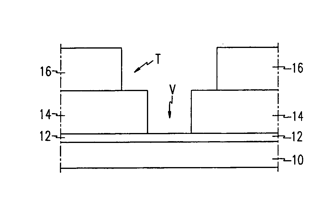
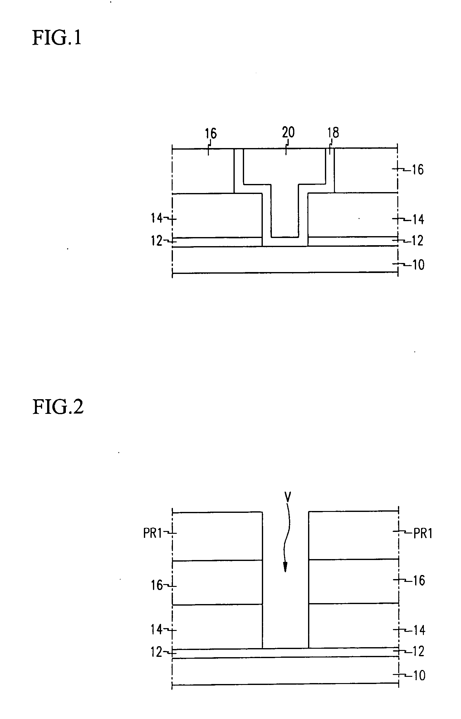
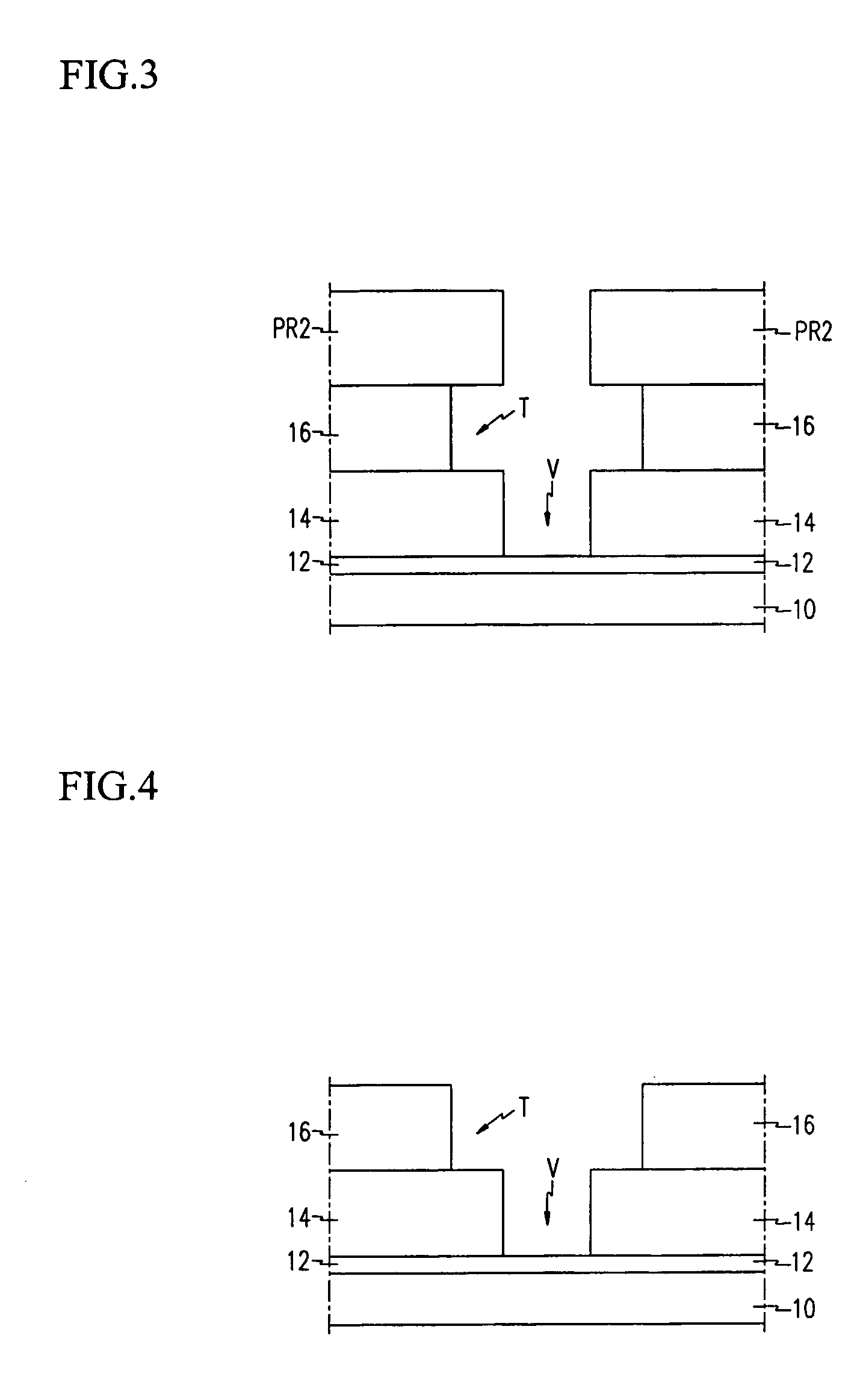
[0016] With reference to the accompanying drawings, the present invention will be described in order those skilled in the art to be able to implement. However, the invention is not limited to the embodiments to be described hereinafter, but, to the contrary, is intended to cover various modification and equivalent arrangements included within the sprit and scope of the appended claims.

[0017] To clarify multiple layers and regions, the thickness of the layers are enlarged in the drawings. Wherever possible, the same reference numbers will be used throughout the drawing(s) to refer to the same or like parts. When it is said any part such as a layer, film, area, or plate is positioned “on” another part, it means the part is right on the other part or above the other part with at least one intermediate part. Further, when it is said that any part is positioned “right on” another part, it means that there is no intermediate part between the two parts (i.e. the parts are in direct contac...


PUM


Abstract

A method for forming a metal wiring of a semiconductor device. The method includes forming an etch stop layer on a semiconductor substrate, forming a first inter metal dielectric on the etch stop layer, and forming a second inter metal dielectric on the first inter metal dielectric. The method also includes forming a first photoresist pattern defining a via hole on the second inter metal dielectric, forming a via hole exposing the etch stop layer using the first photo resist pattern, and forming a second photoresist pattern defining a trench by exposing and developing the first photoresist pattern. The method further includes forming a trench by etching the second inter metal dielectric using the second photoresist pattern as a mask, removing the etch stop layer exposed through the via hole, and forming a metal wiring by filling the via hole and the trench.

Description

BACKGROUND OF THE INVENTION [0001] (a) Field of the Invention [0002] The present invention relates to a method for forming metal wiring of a semiconductor device and, in particular, to a method for forming the metal wiring in a semiconductor device through a dual damascene process. [0003] (b) Description of the Related Art [0004] Recently, as semiconductor devices have become highly integrated and process techniques have been enhanced, conventional aluminum wirings are being replaced by copper wirings for improving the device characteristics, such as operation speed and resistance of the device, and parasitic capacitance between the metals. [0005] However, since the copper has very poor etching characteristics, a damascene process has replaced the conventional etching process. [0006] In the damascene process, a dual damascene pattern having trenches for forming via holes and wirings in an inter metal dielectric is formed, and then a copper layer is deposited thickly enough to fill t...

Claims


Application Information

Patent Timeline
IPC IPC(8): H01L21/28H01L21/4763H01L21/3205H01L21/768H01L23/52H01L29/00
CPCH01L21/76807H01L21/28
Inventor CHO, JOON-YEON
Owner DONGBU ELECTRONICS CO LTD
Why Eureka
Try Eureka