Lithographic apparatus and device manufacturing method

a technology of lithographic apparatus and manufacturing method, which is applied in the direction of electrical apparatus, printers, instruments, etc., can solve the problems of inability to meet the requirements of illumination systems, present lithographic scanners still suffer from high spatial frequency non-uniformities, and inability to achieve high spatial frequency modulation intensity, low cost, and low cost

Active Publication Date: 2005-07-07
ASML NETHERLANDS BV
View PDF1 Cites 27 Cited by
  • Summary
  • Abstract
  • Description
  • Claims
  • Application Information

AI Technical Summary

Benefits of technology

[0038] In an advantageous embodiment of the illumination system according to the invention, the projection beam has a focal point with a minimal cross-sectional area, and the optical element is located at said focal point. Herein, a focal point is to be understood as a position in which the cross-sectional area of the beam is smaller than at exiting the collector, and in certain embodiments, at most half, or more specifically, at most one-

Problems solved by technology

Existing illumination systems, in particular for lithographic apparatus, are not always satisfactory as to the requirement of having a sufficiently homogeneous intensity of the projection beam of radiation.
In particular, present lithographic scanners still suffer from high spatial frequency non-uniformities

Method used


Image

  • Lithographic apparatus and device manufacturing method
  • Lithographic apparatus and device manufacturing method
  • Lithographic apparatus and device manufacturing method

Examples


Embodiment Construction

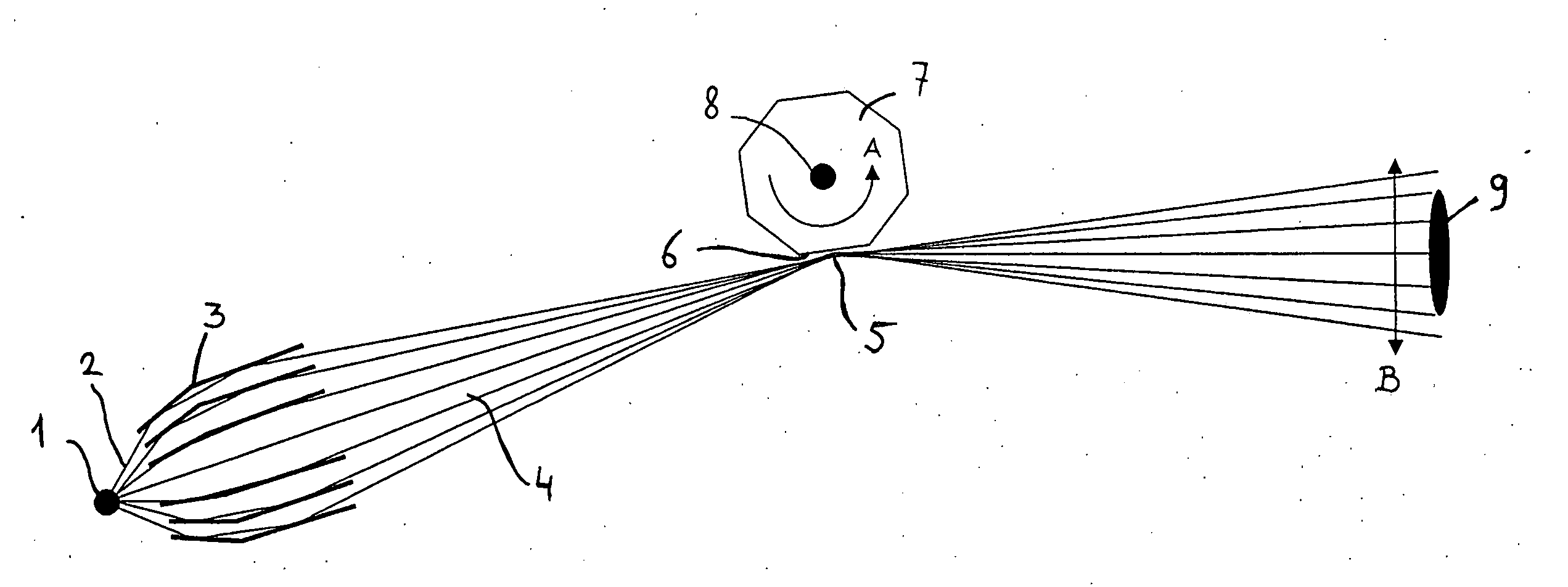
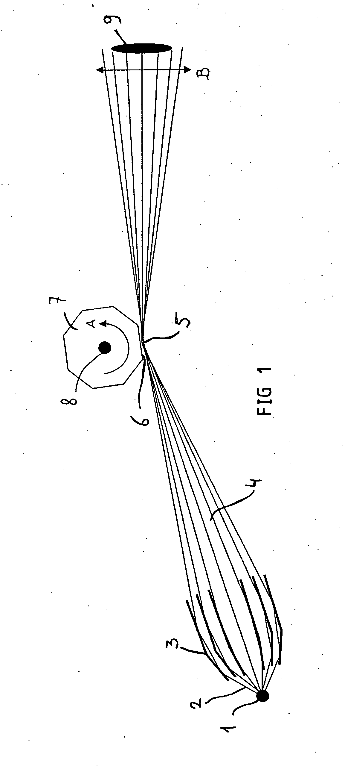
[0067]FIG. 1 schematically depicts an illumination system according to the invention. The illumination system comprises a source 1 of electromagnetic radiation 2. The radiation 2 enters a collector 3 and is formed into a beam 4 of radiation.

[0068] The beam 4 of radiation has a focal point 5, at which it reflects off a face 6 of a polygon 7. The polygon 7 rotates around an axis 8 in the direction indicated by arrow A, and is driven by a motor (not shown).

[0069] The reflected beam oscillates back and forth in the direction of arrow B, and strikes a mirror 9.

[0070] The source 1 may be any source of radiation that is useful for the desired kind of illumination. In many cases this will be electromagnetic radiation, often with wavelengths up to about 1000 nm. In the particular case of lithography, this is most often ultraviolet radiation, having wavelengths from about 400 nm (e.g., 365 nm) down to as short as between 5 and 20 nm (extreme ultraviolet, EUV). In the embodiment of FIG. 1, ...


PUM


Abstract

The present invention provides a lithographic apparatus comprising an illumination system for providing a projection beam of radiation. The illumination system comprises at least one movable optical element (7), such that a projection beam of radiation (4) can be shifted around a central position. This ensures that inhomogeneities in the intensity distribution in the projection beam (4) will be smeared out, which in turn provides an improved homogeneity of the exposure of a surface to be illuminated by the system, such as a wafer or other substrate. The optical element (7) may comprise a motor movable mirror, prism, filter, lens, axicon, diffuser, diffractive optical array, optical integrator, etc. The invention further provides a device manufacturing method, using a lithographic apparatus according to the invention, wherein the optical element is moved, in order to provide an optimum homogeneity for the projection beam of radiation.

Description

[0001] This application claims the benefit of priority from European Patent Application No. 03078463.1, filed Oct. 31, 2003, the entire content of which is incorporated herein by reference. BACKGROUND OF THE INVENTION [0002] 1. Filed of the Invention [0003] The present invention relates to a lithographic apparatus and a device manufacturing method. In particular, the invention relates to a lithographic apparatus comprising an improved illumination system. [0004] 2. Description of the Related Art [0005] Generally, an illumination system is a system for providing a beam of radiation, in order to illuminate an object. Said illumination may be desired for instance in order to be able to view the object, to expose the object to said radiation in order to start or maintain a chemical reaction, and so on. [0006] A known instance of such an illumination system is a slide projector. In a slide projector, as in other illumination systems, it is important that the quality of the beam of radiat...

Claims


Application Information

Patent Timeline
IPC IPC(8): G03B27/54G03F7/20H01L21/027
CPCG03F7/70075
Inventor EURLINGS, MARKUS FRANCISCUS ANTONIUSBASELMANS, JOHANNES JACOBUS MATHEUSBOTMA, HAKOBRUINING, JANDIERICHS, MARCEL MATHIJS THEODORE MARIEDIJSSELDONK, ANTONIUS JOHANNES JOSEPHUS VANSTOELDRAIJER, JUDOCUS MARIE DOMINICUS
Owner ASML NETHERLANDS BV
Why Eureka
Try Eureka