Apparatus for testing a nonvolatile memory and a method thereof

a nonvolatile memory and apparatus technology, applied in the direction of digital storage, grain polishing, instruments, etc., can solve the problems of limited number of chips that can be tested simultaneously, additional address pins are required, and difficult design of control systems

Active Publication Date: 2005-07-07
IXYS INTL LTD
View PDF10 Cites 27 Cited by
  • Summary
  • Abstract
  • Description
  • Claims
  • Application Information

AI Technical Summary

Problems solved by technology

However, due to many connection signals, such control systems have been difficult to design.
In addition, because many channels are used when testing products, there is a limit as to how many chips can be tested simultaneously.
Furthermore, as memory size increases, additional address pins are required.
In addition, because various products have different program and erase times according to certain processes, applying the external clock in certain products may result in the cycle of the external clock being out of synch with programming / erasing methods.

Method used


Image

  • Apparatus for testing a nonvolatile memory and a method thereof
  • Apparatus for testing a nonvolatile memory and a method thereof
  • Apparatus for testing a nonvolatile memory and a method thereof

Examples


Embodiment Construction

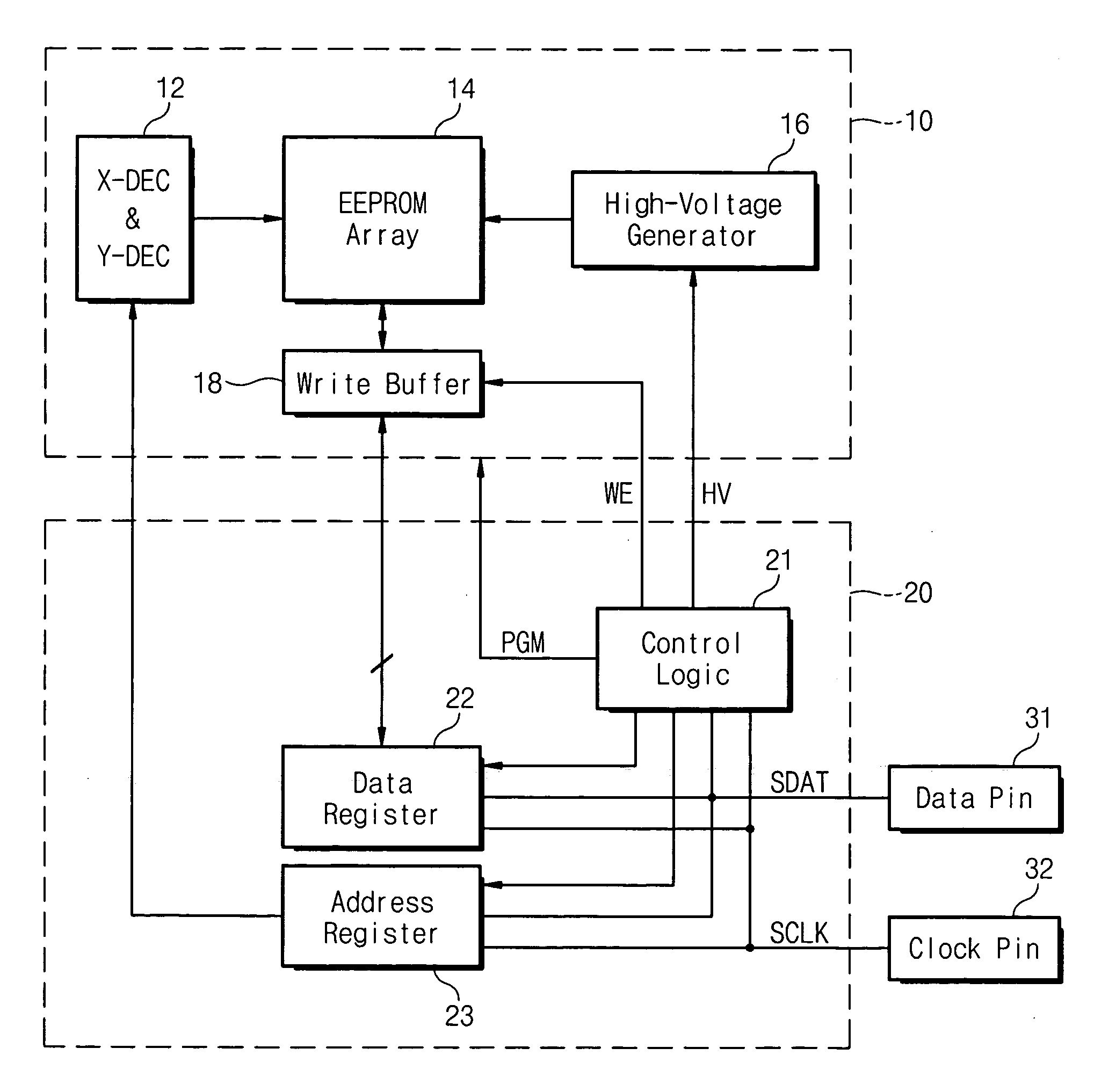
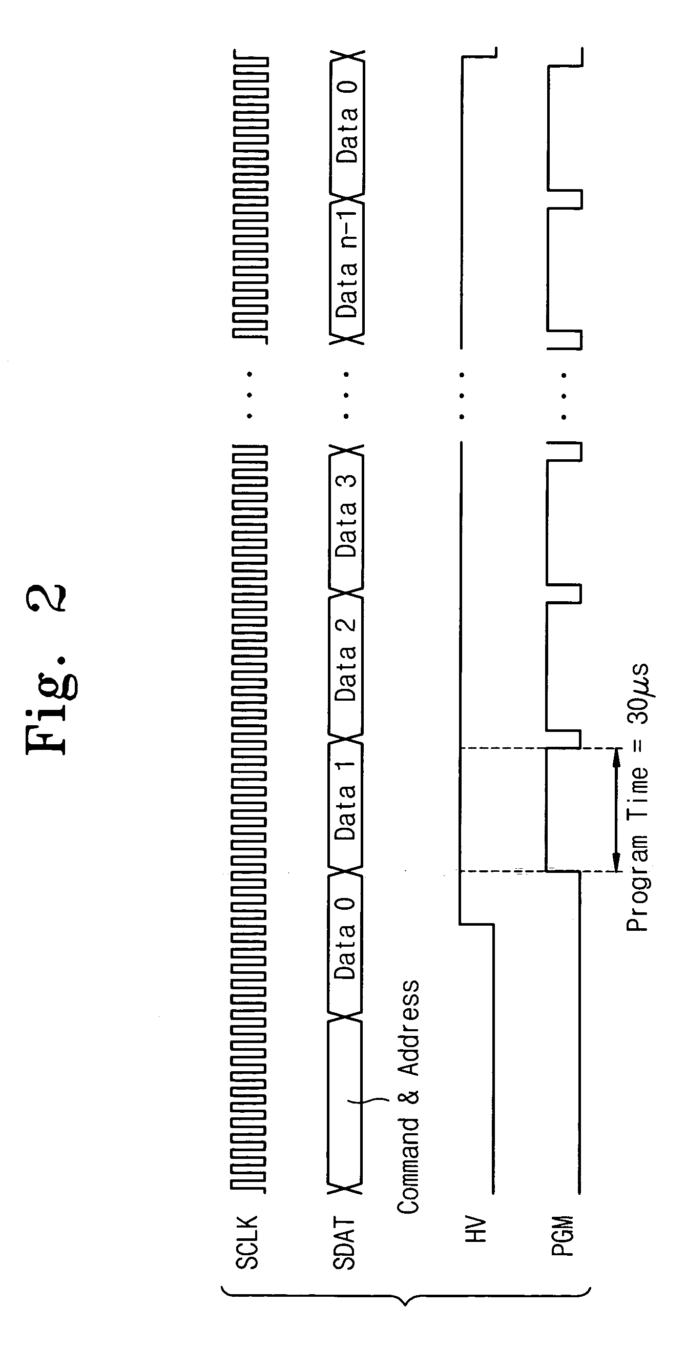
[0023] A transfer protocol for programming a nonvolatile memory embedded in systems employing a clock signal and a data signal, or a sender / receiver data signal may be used by a micro control system (or “a micro controller) according to the present invention. In accordance with the transfer protocol, a data register (or “a serial buffer”) having a size larger than or the same as that of a write buffer in the nonvolatile memory (e.g., 1 Byte through 4 Bytes) is used, and data bits (e.g., 1 Byte through 4 Bytes) required to update storage information are sequentially transferred to the data register from the outside. The transferred data bits are loaded to the write buffer in the nonvolatile memory, and then the loaded data bits are programmed to an array of the nonvolatile memory. While the data bits are programmed, data bits to be programmed next are sequentially transferred to the data register from the outside. Because transferring data and program operations are performed simulta...


PUM


Abstract

An apparatus for testing or programming a nonvolatile memory in a micro control system and a method thereof is provided. The micro control system comprises: a nonvolatile memory for storing data; an address register for storing an address; a data register for storing serial data; control logic for controlling the nonvolatile memory, the address register and the data register; a clock pin for receiving a clock; a data pin for receiving serial data synchronized with the clock; and a timer for measuring time.

Description

FIELD OF THE INVENTION [0001] The present invention relates to semiconductor integrated circuit devices, and specifically, to an apparatus for testing or programming a nonvolatile memory in a micro control system and a method thereof. BACKGROUND [0002] In general, there are two methods for testing nonvolatile memories embedded in micro control systems. One involves testing nonvolatile memories using a parallel interface, and the other involves testing nonvolatile memories using a serial interface. [0003] When testing nonvolatile memories using a parallel interface, an independent memory chip of a nonvolatile memory can be controlled employing addresses, data and control signals. However, due to many connection signals, such control systems have been difficult to design. In addition, because many channels are used when testing products, there is a limit as to how many chips can be tested simultaneously. Furthermore, as memory size increases, additional address pins are required. [000...

Claims


Application Information

Patent Timeline
Patent Type & Authority Applications(United States)
IPC IPC(8): G06F11/22G11C11/34G11C29/00G11C29/48
CPCG11C29/003G11C2029/0401G11C29/48G11C29/1201B02B3/06B02B5/02B02B7/02
Inventor AHN, JONG-KEUN
Owner IXYS INTL LTD
Why Eureka
Try Eureka