

Method of varying etch selectivities of a film
a technology of etch selectivity and film, which is applied in the field of patterning of crystalline films, can solve the problems of poor pattern fidelity between the mask pattern and the limit the ability to further scale the etch selectivity of crystalline films
- Summary
- Abstract
- Description
- Claims
- Application Information
AI Technical Summary
Problems solved by technology
Method used
Image

Examples
Embodiment Construction
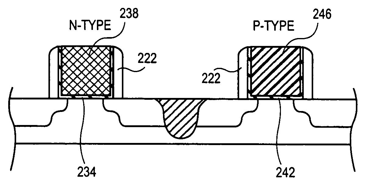
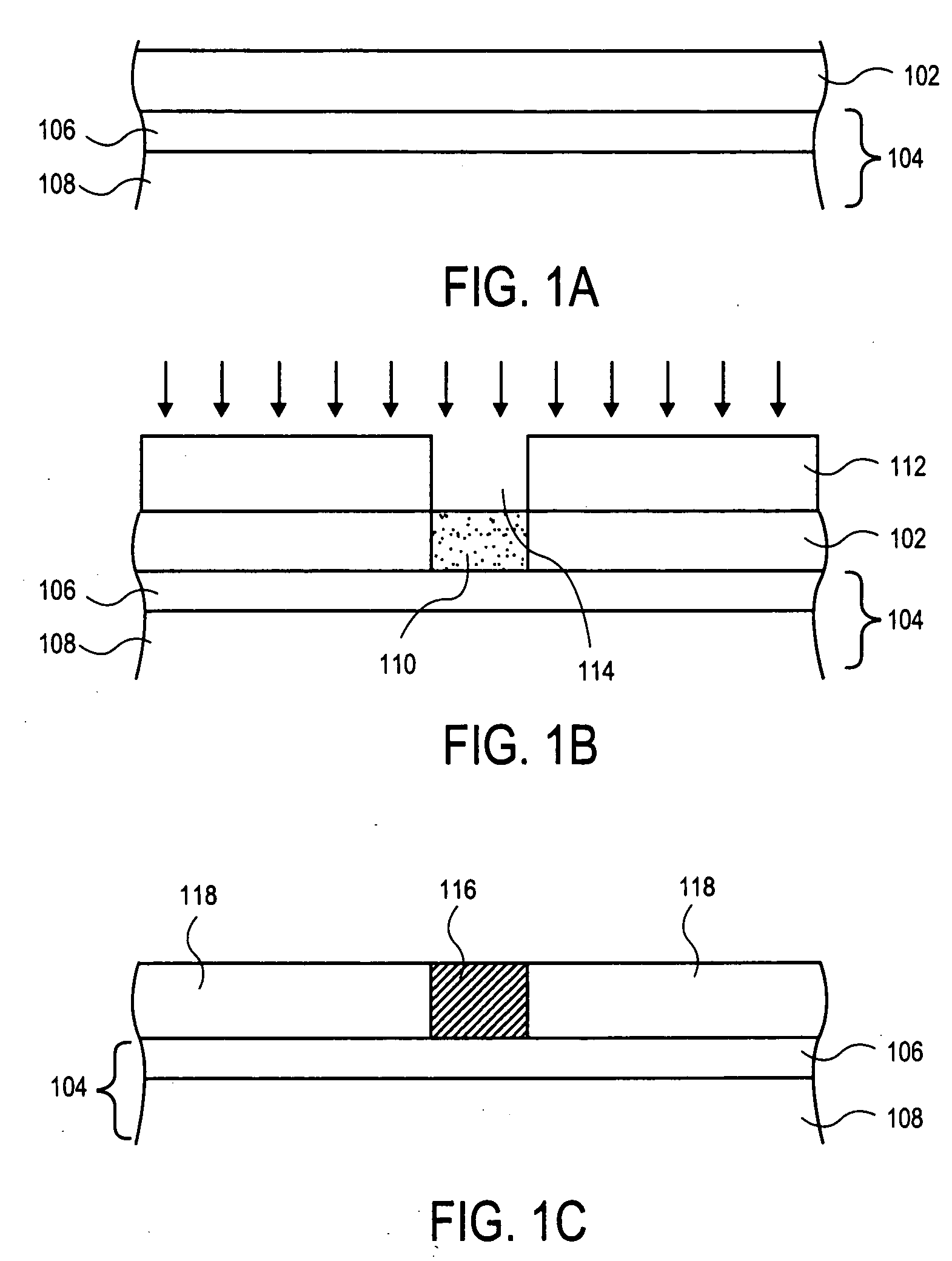
[0008] A method of varying the etch selectivity of a crystalline film is described. In the following description numerous specific details are set forth in order to provide a thorough understanding of the present invention. In other instances, well known semiconductor processing techniques and features have not been described in particular detail in order to not unnecessarily obscure the present invention.
[0009] The present invention is a method to alter the etch selectivity of crystalline films by modifying the lattice energy of the film. According to the present invention, a crystalline film to be etched is provided. The crystalline film has symmetrical lattice or a “degenerate” lattice. Dopant atoms are then placed into a portion of the crystalline film and the film heated to a sufficient energy to cause the dopants to substitute with atoms in the crystalline film. Utilizing dopant atoms which have a sufficiently different size than the atoms of the crystalline film causes a dis...
PUM
 Abstract
Description
Claims
Application Information