

Multilayer wiring board including stacked via structure
a wiring board and via technology, applied in the direction of printed circuit aspects, sustainable manufacturing/processing, final product manufacturing, etc., can solve the problem of cracking in the connection between the filled vias, and achieve the effect of excellent reliability
- Summary
- Abstract
- Description
- Claims
- Application Information
AI Technical Summary
Benefits of technology
Problems solved by technology
Method used
Image

Examples
Embodiment Construction
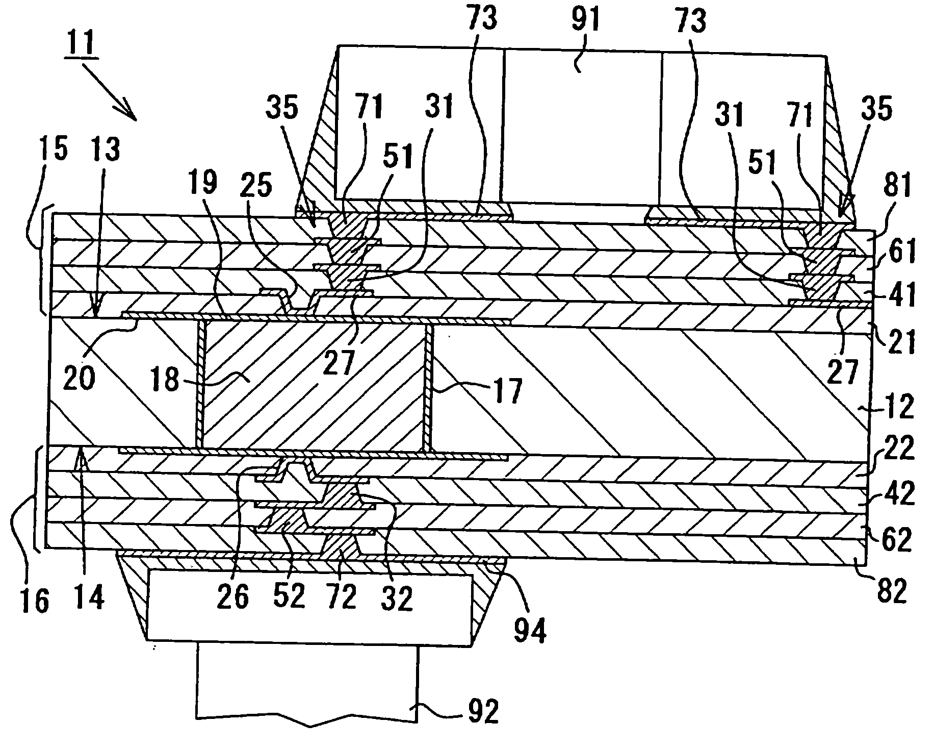
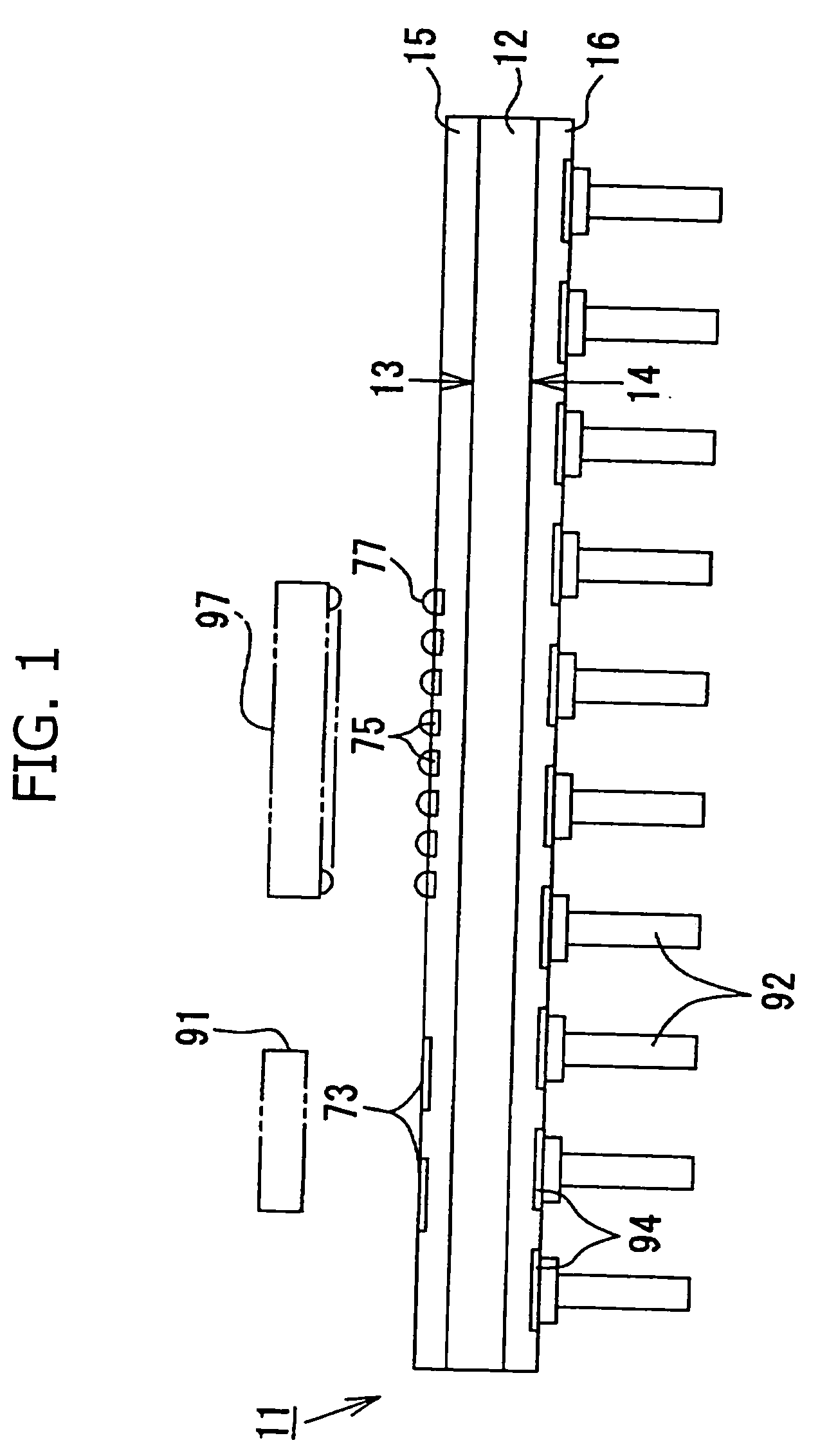
[0043] A “build-up” multilayer wiring board, generally denoted 11, as constructed according to one embodiment of the present invention, will now be described in detail with reference to FIGS. 1 to 9.
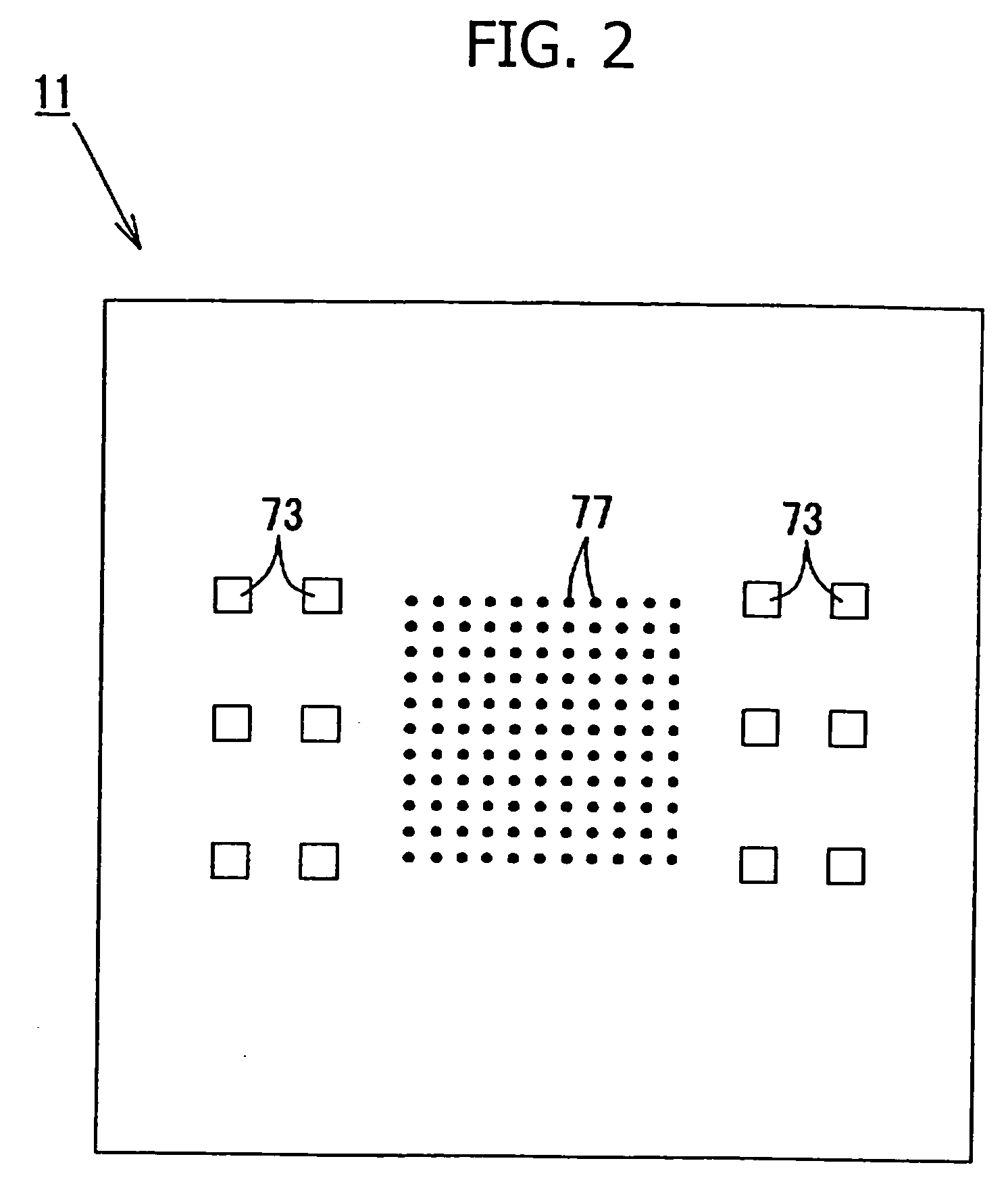
[0044] As shown in FIGS. 1 to 3, the multilayer wiring board 11 of this embodiment includes, in this implementation, a substantially rectangular substrate 12 as a core or base material. In a specific non-limiting implementation, the substrate 12 is formed of BT resin and has a thickness of about 600 μm to 800 μm. As shown in FIG. 3, an upper “build-up” layer 15 is formed on an upper surface (i.e., a first main surface) 13 of the substrate 12, and a lower “build-up” layer 16 is formed on a lower surface (i.e., a second main surface) 14 of the substrate 12. A number of plated through holes 17, typically having a diameter of about 200 μm to 300 μm, are formed in the substrate 12 at predetermined positions in such a manner as to extend through the substrate 12 between the upper surface 13 a...
PUM
 Abstract
Description
Claims
Application Information