Methods, systems and computer program products for dynamically controlling a semiconductor dicing saw

a technology of dynamic control and dicing saw, which is applied in the field of manufacturing of semiconductor devices, can solve the problems of high cost, complicated sawing, and slow individual semiconductor devices, and achieve the effect of reducing the time required to dice a wafer and improving the throughput of the wafer

Inactive Publication Date: 2005-07-21
CREE INC
View PDF0 Cites 0 Cited by
  • Summary
  • Abstract
  • Description
  • Claims
  • Application Information

AI Technical Summary

Benefits of technology

[0008] Accordingly, there is a need in the art for controlling a semiconductor dicing saw in a manner that may decrease the time required to dice a wafer and / or may improve wafer throughput in the semiconductor device manufacturing process.

Problems solved by technology

Individual semiconductor devices are typically extremely small compared to the size of the wafer on which they are formed.
Sawing may be a slow, laborious task that is typically performed using expensive, complicated saws.
All of these factors tend to make dicing a time-consuming bottleneck in the semiconductor device fabrication process.

Method used


Image

  • Methods, systems and computer program products for dynamically controlling a semiconductor dicing saw
  • Methods, systems and computer program products for dynamically controlling a semiconductor dicing saw
  • Methods, systems and computer program products for dynamically controlling a semiconductor dicing saw

Examples


Embodiment Construction

[0028] The present invention now will be described more fully hereinafter with reference to the accompanying drawings, in which embodiments of the invention are shown. This invention should not be construed as limited to the embodiments set forth herein; rather, these embodiments are provided so that this disclosure will be thorough and complete, and will fully convey the scope of the invention to those skilled in the art. Like numbers refer to like elements throughout. Furthermore, the various layers and regions illustrated in the figures are illustrated schematically. As will also be appreciated by those of skill in the art, while the present invention is described with respect to semiconductor wafers and diced chips, such chips may be diced into arbitrary sizes. Accordingly, the present invention is not limited to the relative size and spacing illustrated in the accompanying figures.

[0029] As will be appreciated by one of skill in the art, the present invention may be embodied a...


PUM

PropertyMeasurementUnit
diameteraaaaaaaaaa
diameteraaaaaaaaaa
diameteraaaaaaaaaa

Abstract

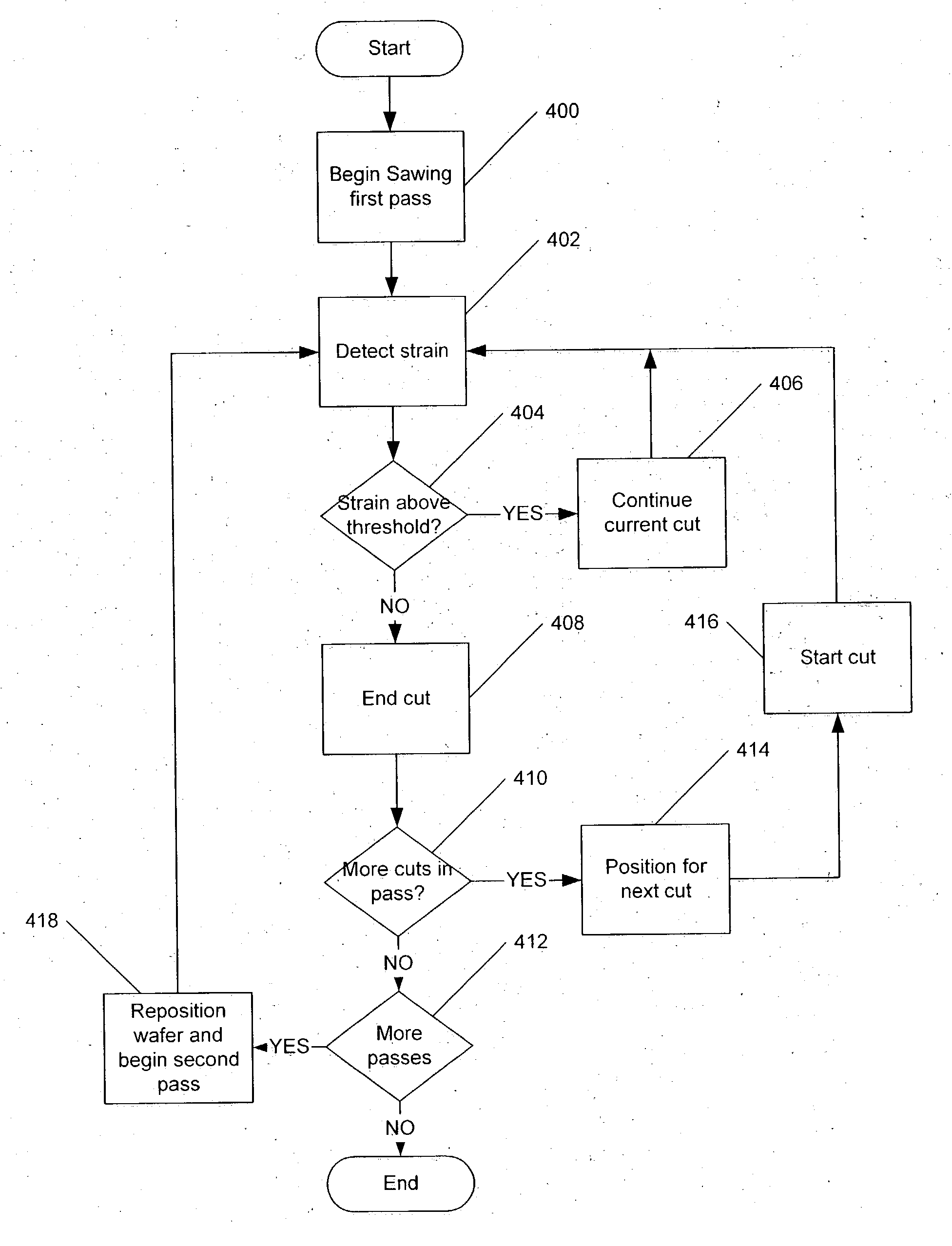
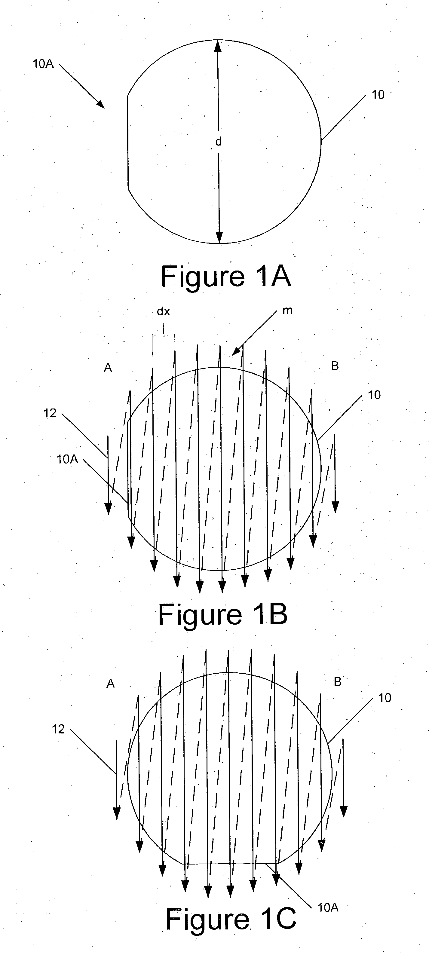
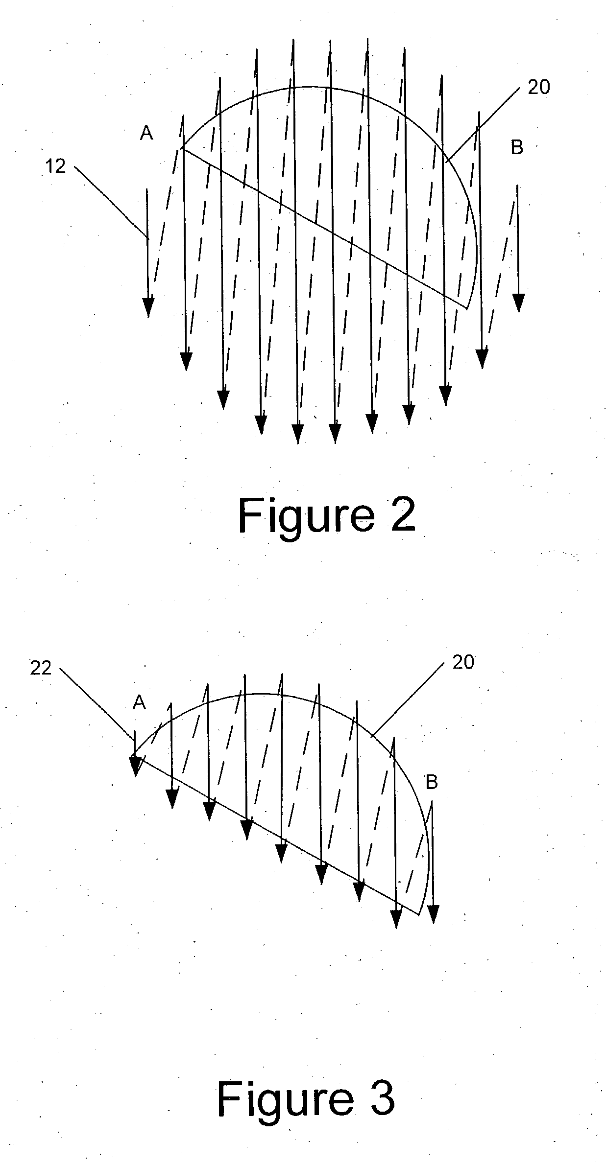
A saw cutting pattern is dynamically established for a semiconductor dicing saw based on detection of the saw blade contacting a wafer or a portion of a wafer. The dynamic cutting pattern may terminate cuts if the saw blade no longer contacts the wafer or a portion of a wafer. Thus, irregular shaped wafers may be cut without requiring that an entire predefined cutting pattern be carried out and/or without previously mapping the shape of the wafer or portion of a wafer. A map of the wafer or a portion of a wafer may also be generated based on the detection of the saw blade contacting the wafer during a first cutting pass and may be used during a second cutting pass.

Description

RELATED APPLICATIONS [0001] The present application is related to and claims priority from U.S. provisional application Ser. No. 60 / 398,753, filed Jul. 26, 2003 and entitled “Methods, Systems and Computer Program Products for Controlling a Semiconductor Dicing Saw,” the disclosure of which is incorporated herein as if set forth in its entirety.FIELD OF THE INVENTION [0002] The present invention relates to fabrication of semiconductor devices, and in particular to dicing wafers into individual components by means of a dicing saw. BACKGROUND [0003] Semiconductor devices are typically fabricated on a substrate that provides mechanical support for the device and often contributes to the electrical performance of the device as well. Silicon, germanium, gallium arsenide, sapphire and silicon carbide are some of the materials commonly used as substrates for semiconductor devices. Many other materials are also used as substrates. Semiconductor device manufacturing typically involves fabrica...

Claims


Application Information

Patent Timeline
Patent Type & Authority Applications(United States)
IPC IPC(8): B28D5/00
CPCB28D5/0064
Inventor HUBBELL, EDWARD J. III
Owner CREE INC
Why Eureka
Try Eureka